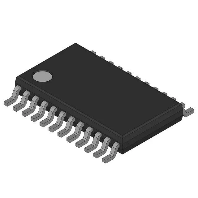
24-TSSOP footprint and supply rails
The CY2PD817ZC: The differential input (LVPECL) and differential output paths mean the PCB traces between the source and the seven fanout loads must be impedance-controlled (50 Ω single-ended, 100 Ω differential) and length-matched to within the skew budget of the downstream receivers.
Active production — what that means for a BOM line
Infineon lists the CY2PD817ZC as active. RoHS non-compliant — the lead finish on the 24-TSSOP package is likely SnPb. If your assembly line runs only Pb-free profiles, this part requires a segregated solder paste and a reflow temperature ceiling that matches the SnPb alloy (typically 210-220 °C peak).
320 MHz ceiling and the 1:7 fanout
Rated for 320 MHz maximum frequency, this low-skew clock driver distributes one LVPECL input to seven outputs that can be individually configured as LVCMOS, LVPECL, or LVTTL. The differential input and differential output paths mean the part preserves the signal integrity of a high-speed clock across the fanout tree. For a 320 MHz clock, the output rise time into a 10 pF load determines the usable trace length more than the bare frequency spec.