1:8 fanout buffer — 350 MHz ceiling, differential path
The CY2DP818ZI is a low-skew clock driver from Infineon, a 1:8 fanout buffer that takes a single differential or single-ended input and delivers eight matched LVPECL outputs. The 350 MHz maximum frequency covers most PCIe reference clock, Ethernet SerDes, and FPGA global clock distribution requirements — the 1:8 ratio means one oscillator or PLL output fans out to eight loads without adding a second buffer stage. The input accepts LVDS, LVPECL, or LVTTL levels, and the output is always LVPECL. The differential-through path (Yes/Yes) preserves signal integrity across the fanout: the common-mode rejection of the LVPECL output stage attenuates ground-bounce and supply noise that would otherwise couple into the clock tree.
Supply rails and temperature grade
The supply range is 3.135 V to 3.465 V — a tight 3.3 V ±5 % window. The single-circuit (Number of Circuits: 1) means one input drives all eight outputs — there is no second independent buffer channel on the die. The 1:8 ratio is the fanout count; the input-to-output skew is the spec that matters for parallel clock trees, though the datasheet's low-skew claim signals the part was characterised for matched propagation delays across the eight lanes.
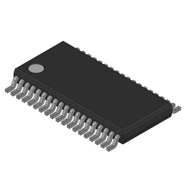
The CY2DP818ZI is supplied in a 38-TFSOP (0.173", 4.40 mm width) package, also designated as the 38-TSSOP supplier device package. The 0.5 mm pitch TSSOP footprint is a standard layout; the narrow body (4.4 mm) keeps the pin-to-pin trace length short for the LVPECL outputs, which need controlled-impedance routing (50 Ω to VTT - 2 V termination). The surface-mount package reflows on a standard lead-free profile — no special handling beyond the usual moisture sensitivity level bake. For a prototype run or a small production batch this is convenient — no reel fee, no minimum reel quantity. For high-volume pick-and-place, a reeled variant would be the standard choice; confirm the packaging preference with the BOM line.
The RoHS compliance status is listed as non-compliant. This means the part does not meet the EU RoHS directive — likely due to lead content in the solder balls or die-attach material. For RoHS-exempt applications (military, aerospace, certain industrial and medical equipment with exemption 7(c)-I), this is acceptable. For standard commercial or consumer products that require full RoHS compliance, a lead-free variant should be sourced.