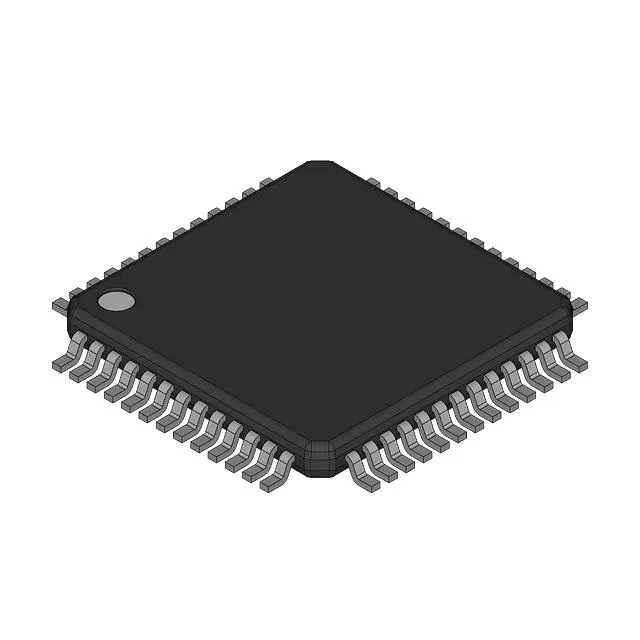
Infineon Technologies CY29972AIT — Clock & Timing ICs

CY29972AIT clock generator, 125 MHz, 52-LQFP

MPNCY29972AIT
End of Life

Cypress CY29972AIT clock generator, Fanout Distribution / Multiplexer / Spread Spectrum Clock Generator / Zero Delay Buffer, PLL Yes with Bypass, 125 MHz max, 3:12 input:output, 2.9V–3.6V supply, -40°C to 85°C, 52-LQFP (10x10 mm), Surface Mount.

$6.45Ref. price · indicative, final on quote
Packaging52-LQFP
StockContact for availability
MOQ1 pcs
  • 100% new & originalTraceable channels only — no refurbs, no pulls, no remarked parts.
  • Date & lot codes on quoteStated per line before you commit; label photos on request.
  • MSL-compliant ESD packingMoisture-sealed bags with indicator cards; reels photo-verified.
  • PayPal buyer protectionPay by T/T, PayPal or Payoneer — card payments covered end to end.

Specifications

CY29972AIT Technical Specifications
ParameterValue
TypeFanout Distribution, Multiplexer, Spread Spectrum Clock Generator, Zero Delay Buffer
Mounting typeSurface Mount
Voltage2.9V ~ 3.6V
Frequency125MHz
Operating temperature-40°C ~ 85°C
PLLYes with Bypass
InputClock, Crystal
OutputClock
PackageBulk
Case52-LQFP
Divider (Multiplier)Yes/No
Number of circuits1
Ratio - Input:Output3:12
Differential - Input:OutputNo/No

Product details

Clock distribution in a single 52-pin package

The Cypress CY29972AIT is a multi-function clock device that combines fanout distribution, a multiplexer, a spread-spectrum clock generator, and a zero-delay buffer in one 52-LQFP package. It accepts either a clock or crystal input and delivers up to twelve clock outputs from three inputs, with a PLL that includes a bypass mode. The 125 MHz maximum frequency and 2.9 V to 3.6 V supply range make it suited for board-level clock trees in telecom, networking, and industrial equipment where multiple clean clock domains are needed from a single reference.

125 MHz ceiling and PLL bypass — what they mean on the board

The 125 MHz maximum output frequency covers common Ethernet, PCIe reference, and FPGA fabric clocks. The PLL with bypass lets you run the outputs directly from the input when jitter performance matters more than frequency multiplication — useful for test modes or low-jitter paths. The 3:12 input-to-output ratio means you can feed three independent clock sources and distribute them to twelve loads, reducing the number of discrete buffers and oscillators on the bill of materials.

Industrial temperature and supply tolerance

Rated for -40°C to 85°C operation, the CY29972AIT fits outdoor telecom cabinets, factory-floor controllers, and engine-bay-adjacent electronics without derating. The 2.9 V to 3.6 V supply window tolerates 3.3 V rails with ±10% margin, including the drop across a long PCB trace or a lightly loaded LDO.

Lifecycle and compliance

Note that this part is RoHS non-compliant (per the supplier listing), so it is not suitable for assemblies requiring RoHS exemption-free status.

Frequently asked questions

Is CY29972AIT RoHS compliant?

No, the supplier lists it as RoHS non-compliant. Verify your assembly's exemption policy before specifying.

What is the closest functional equivalent to CY29972AIT?

The CY2305SXI-1HT is a zero-delay buffer with a similar function but a 1:5 input-to-output ratio and a 133.33 MHz maximum, in a smaller package. It is not a pin-for-pin replacement; review the ratio and package differences for your design.