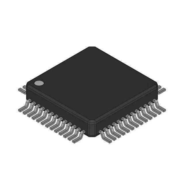
Infineon Technologies CY29949AC — Analog & Data Acquisition

CY29949AC Low Skew Clock Driver, 200 MHz, 52-TQFP

MPNCY29949AC
End of Life

Cypress CY29949AC, Low Skew Clock Driver, Fanout Buffer (Distribution) / Divider / Multiplexer, 200 MHz max, 2:15 I/O, LVCMOS/LVPECL/LVTTL input, LVCMOS/LVTTL output, 52-TQFP, 0°C to 70°C.

$2.49Ref. price · indicative, final on quote
Packaging52-TQFP
StockContact for availability
MOQ1 pcs
  • 100% new & originalTraceable channels only — no refurbs, no pulls, no remarked parts.
  • Date & lot codes on quoteStated per line before you commit; label photos on request.
  • MSL-compliant ESD packingMoisture-sealed bags with indicator cards; reels photo-verified.
  • PayPal buyer protectionPay by T/T, PayPal or Payoneer — card payments covered end to end.

Specifications

CY29949AC Technical Specifications
ParameterValue
TypeFanout Buffer (Distribution), Divider, Multiplexer
Mounting typeSurface Mount
Voltage2.375V ~ 2.625V, 2.97V ~ 3.63V
Frequency200 MHz
Operating temperature0°C ~ 70°C
InputLVCMOS, LVPECL, LVTTL
OutputLVCMOS, LVTTL
PackageBulk
Case52-TQFP
Number of circuits1
Ratio - Input:Output2:15
Differential - Input:OutputYes/Yes

Product details

200 MHz low skew fanout — what it buys the clock tree

The Cypress CY29949AC is a low skew clock driver combining fanout buffer, divider, and multiplexer functions in one 52-TQFP package. It accepts LVCMOS, LVPECL, or LVTTL inputs and delivers LVCMOS or LVTTL outputs at frequencies up to 200 MHz, with differential I/O capability throughout. The 2:15 input-to-output ratio lets a single device replace multiple smaller fanout buffers, saving board area and reducing skew accumulation in multi-drop clock trees. Supply voltage operates from either 2.375 V to 2.625 V or 2.97 V to 3.63 V, covering common 2.5 V and 3.3 V logic rails.

Differential I/O and mixed-signal clock trees

Because both input and output paths are rated differential (Yes/Yes per the spec), the CY29949AC can accept a clean LVPECL reference from an oscillator and distribute LVCMOS copies to multiple ASICs or FPGAs without an extra level translator. The integrated divider and multiplexer also allow clock-frequency scaling or source selection on the same die — useful for systems that switch between a primary and redundant clock source.

RoHS non-compliance — check your market

The CY29949AC is listed as RoHS non-compliant. For designs shipping into EU or other RoHS-regulated regions, this part requires an exemption or a leaded-solder process. If your BOM requires RoHS compliance, a lead-free equivalent in the same Cypress clock-driver family would be the appropriate cross-shop.

Package and temperature grade

Housed in a 52-TQFP (10x10 mm) with surface-mount footprint, the part is rated for commercial temperature range (0°C to 70°C). That limits it to indoor, temperature-controlled environments — not suitable for industrial or automotive under-hood use without extended-range qualification.

Frequently asked questions

What is the maximum frequency of CY29949AC?

The device supports a maximum output frequency of 200 MHz across its LVCMOS/LVTTL outputs.

What input voltage range does CY29949AC accept?

The supply voltage range is 2.375 V to 2.625 V (2.5 V rail) or 2.97 V to 3.63 V (3.3 V rail). Input logic levels are LVCMOS, LVPECL, or LVTTL.