PLL with bypass — one device, three clock-tree roles
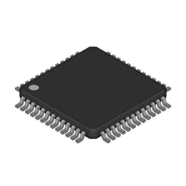
The CY29773AI integrates a PLL that can be bypassed, letting the part serve as a zero-delay buffer (PLL locked), a clean fanout distribution amplifier (PLL cleaning jitter), or a simple multiplexer (PLL bypassed). This means a single BOM line covers three distinct clock-tree functions — useful when the same PCB must support multiple speed grades or when the clock source changes between production runs. The 4:12 input-to-output ratio means one active LVCMOS or LVPECL input fans out to 12 LVCMOS clock lines. The three spare input pins can be tied off or used as redundant clock sources with automatic failover if the primary input drops.
200 MHz ceiling, single-ended I/O — know the speed and signal-type limits
The 200 MHz maximum frequency sets the output clock ceiling. Below that, the PLL can multiply the input frequency (divider/multiplier: Yes/No) up to the 200 MHz limit, but the part cannot generate a differential output — all 12 outputs are single-ended LVCMOS, so it is not a fit for PCIe, SATA, or 10GbE reference clocks that require LVPECL or HCSL levels. The dual supply range (2.375-2.625 V and 3.135-3.465 V) means the core and I/O run on separate rails. The PCB must route both supply planes; a missing 2.5 V rail will leave the PLL core unpowered even if the 3.3 V I/O rail is present.
Active production, RoHS non-compliant — legacy BOM fit
Supplied by Infineon Technologies.