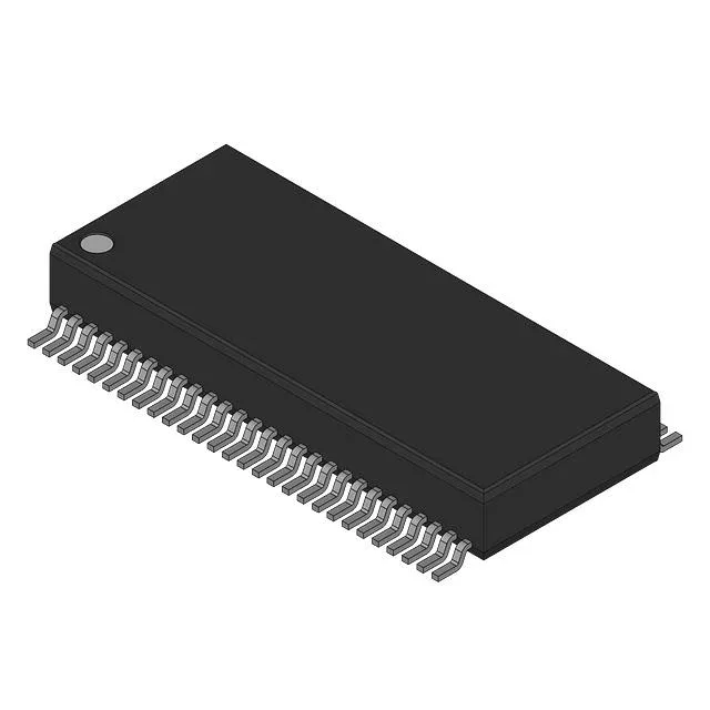
Chipset-targeted DDR clock generator
The CY28341OC-3T is a PLL-based clock generator designed specifically for the VIA P4/KT/KM400A chipset family — the part number suffix and the description string confirm this is not a general-purpose clock buffer but a chipset-specific frequency timing generator (FTG). It accepts a crystal input and produces up to 20 clock outputs at a maximum frequency of 200 MHz, with differential outputs (No/Yes) meaning the DDR memory controller receives LVDS-style clock pairs, not single-ended rails. The dual supply range — 2.375 V for the core PLL and 3.135 V for the I/O — means both rails must be present and within tolerance for the PLL to lock; a missing or out-of-spec rail will hold the outputs in tristate or produce an unlocked clock.
Lifecycle and compliance
RoHS non-compliant — the part contains lead or other restricted substances per the original manufacturing date. This blocks EU RoHS markets unless an exemption (e.g., for high-reliability or leaded solder exemption) applies. Confirm local regulatory acceptance before specifying.