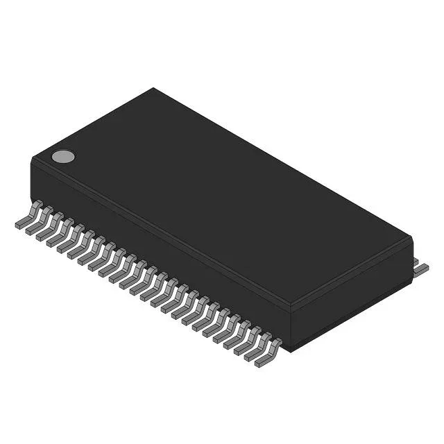
PLL-based spread-spectrum clock generator — 1:19 fanout, dual supply
The CY28325OC-3 is a PLL-based spread-spectrum clock generator. It accepts either an LVTTL reference or a crystal input and produces up to 19 clock outputs from that single source — a 1:19 input-to-output ratio. The spread-spectrum modulation spreads the output energy across a wider frequency band, reducing peak EMI radiated from the clock traces and cables in a system. The device operates from two independent supply rails: 2.375 V to 2.625 V and 3.135 V to 3.465 V. The maximum output frequency is 1 MHz, so this part is suited for distributing lower-speed clocks (system reference, audio frame sync, microcontroller clock trees) rather than high-speed SERDES or memory interfaces.
Package, temperature grade, and differential signaling
Housed in a 48-BSSOP (0.295", 7.50 mm width) surface-mount package, also listed as supplier device package 48-SSOP. The 0.65 mm pin pitch is standard for this body width — layout engineers should match the footprint to the SSOP-48 land pattern in their CAD library. Both the input and output paths are single-ended only — differential input is No and differential output is No. That means the clock distribution uses standard LVTTL traces with 50-ohm series termination at the source, not differential pairs with 100-ohm routing. The divider/multiplier function is present (Yes), but there is no internal multiplier (No) — the PLL multiplies the reference internally, but a separate multiplier block is not exposed. One circuit, one PLL core.
Active lifecycle, RoHS non-compliant — legacy BOM fit
However, it is marked RoHS non-compliant, meaning the termination finish contains lead (likely SnPb or similar). This part fits legacy BOMs that require tin-lead solder for rework or reliability reasons, or designs that are exempt from RoHS (military, aerospace, medical implant). New RoHS-compliant designs should check the CY28325OC-3's lead-free variant or a pin-compatible replacement.