PLL with bypass — what the feature actually does
The CY28324PVCT: The integrated PLL generates a clean, multiplied clock from the LVTTL input, and the bypass mode lets you feed the reference clock straight through when you do not need frequency synthesis — useful during system bring-up or when the downstream device needs the raw input rate. With a 1:8 input-to-output ratio, a single reference clock fans out to eight clock outputs, covering the distribution needs of a typical multi-IC board without an external fan-out buffer.
The 48 MHz maximum output frequency suits common microcontroller, memory, and peripheral clock domains — anything above that needs a faster PLL or a different part. Supply range is 3.135 V to 3.465 V, which is the standard 3.3 V ±5 % rail found on most digital boards; no extra regulator or level shifting is needed if your board already runs 3.3 V logic.
Package and board-fit — 48-BSSOP
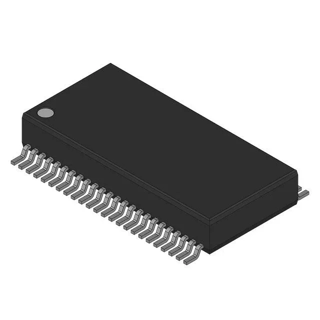
Housed in a 48-BSSOP (0.295", 7.50 mm width) package, also listed as 48-SSOP — the 0.025-inch lead pitch is fine for a two-layer board but benefits from a four-layer stack for signal integrity on the eight clock outputs. Surface-mount assembly with a standard SSOP footprint; no exposed pad to solder, so reflow profile follows the standard JEDEC for 48-pin SSOP packages.
Temperature grade and deployment envelope
The differential output is listed as No on the input side and Yes on the output side, meaning the clock outputs are differential (likely LVDS or similar) while the input is single-ended LVTTL — check the output termination for the differential pair on the board layout.