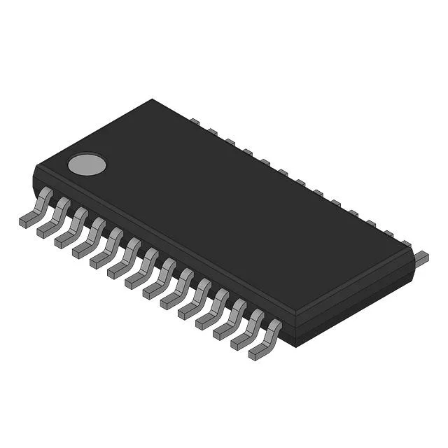
25 ns access UV EPROM for legacy 5V firmware storage
The CY27H256-25ZC is a 256Kbit UV-erasable EPROM organized as 32K x 8 bits, with a 25 ns maximum access time. The 25 ns access time sets the read-cycle window for the host CPU or logic — the memory must present valid data within that window from address assertion, which constrains bus timing margins in legacy 5V processor designs.
UV-EPROM technology and package
This device uses UV-EPROM technology, meaning the die is erased by exposure to ultraviolet light through a quartz window in the package. In production, the device is programmed once and treated as a one-time-programmable (OTP) memory — field erasure requires a UV eraser and is practical only during development or rework. The 28-TSOP I package (0.465" body width, 11.80 mm) is a surface-mount thin small-outline package. The windowed variant allows UV erasure; the non-windowed OTP version is a separate order code. The 28-TSOP I footprint is standard for byte-wide EPROMs of this era and density. The commercial temperature grade (0°C to 70°C) limits deployment to indoor, temperature-controlled environments — not suitable for industrial or automotive ambient extremes without additional qualification data.
Active lifecycle and compliance note
RoHS non-compliant (lead-bearing construction). This is typical for UV-EPROM devices that use a windowed ceramic or plastic package with a lead-frame finish that does not meet the RoHS exemption sunset. Designs requiring RoHS compliance should evaluate the non-windowed OTP variant or a serial-flash migration path.