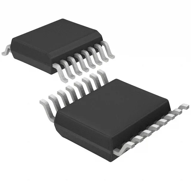
Infineon Technologies CY23S09ZXC-1H — Clock & Timing ICs

Infineon CY23S09ZXC-1H Clock ZDB, 133MHz, 16-TSSOP

MPNCY23S09ZXC-1H
End of Life

Infineon CY23S09ZXC-1H zero delay buffer, 1:9 fanout, 133.33 MHz max, LVCMOS I/O, PLL with bypass, 3V-3.6V supply, 16-TSSOP.

$11.3Ref. price · indicative, final on quote
Packaging16-TSSOP (0.173", 4.40mm Width)
Independent supplier — new & surplus stockAuthenticity-screened · ESD-safe packingListing updated Aug 2026

Specifications

CY23S09ZXC-1H specifications
ParameterValue
TypeFanout Buffer (Distribution), Zero Delay Buffer
MountingSurface Mount
Voltage3V ~ 3.6V
Frequency133.33MHz
Operating temperature0°C ~ 70°C
PLLYes with Bypass
InputLVCMOS, LVTTL
OutputLVCMOS
PackageBulk
Case16-TSSOP (0.173\", 4.40mm Width)
Divider (Multiplier)No/No
Number of circuits1
Ratio - Input:Output1:9
Differential - Input:OutputNo/No

Product details

The CY23S09ZXC-1H is a zero delay buffer with a 1:9 fanout ratio, designed to distribute a single LVCMOS or LVTTL input clock to nine LVCMOS outputs while maintaining phase alignment. The integrated PLL includes a bypass mode, allowing the input clock to pass directly to the outputs when the PLL is not required for zero-delay synchronization. Maximum output frequency is 133.33 MHz, making it suitable for clock distribution in systems with moderate-speed digital logic, such as FPGAs, ASICs, or memory controllers.

Rated for the commercial temperature range of 0°C to 70°C, which covers most indoor equipment, networking gear, and test instrumentation — but not extended industrial or automotive environments.

Frequently asked questions

What is the maximum operating frequency of this zero delay buffer?

The CY23S09ZXC-1H supports a maximum output frequency of 133.33 MHz, with a 1:9 fanout from a single LVCMOS or LVTTL input.