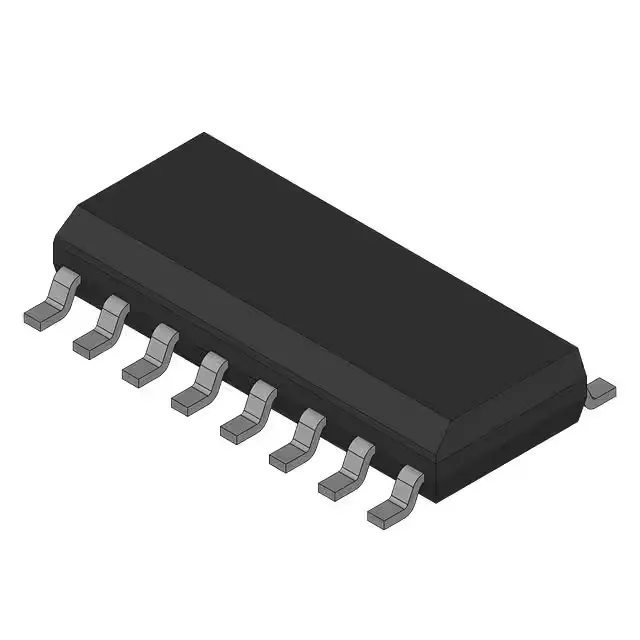
Infineon Technologies CY23S08SC-4 — Clock & Timing ICs

CY23S08SC-4 Clock Buffer

MPNCY23S08SC-4
End of Life

Infineon Technologies CY23S08SC-4, PLL-based zero delay buffer, 1:8 LVCMOS fanout, 140 MHz max, 16-SOIC surface mount, 3 V to 3.6 V supply, commercial temperature range.

$1.25Ref. price · indicative, final on quote
Packaging16-SOIC (0.154", 3.90mm Width)
StockContact for availability
MOQ1 pcs
  • 100% new & originalTraceable channels only — no refurbs, no pulls, no remarked parts.
  • Date & lot codes on quoteStated per line before you commit; label photos on request.
  • MSL-compliant ESD packingMoisture-sealed bags with indicator cards; reels photo-verified.
  • PayPal buyer protectionPay by T/T, PayPal or Payoneer — card payments covered end to end.

Specifications

CY23S08SC-4 Technical Specifications
ParameterValue
TypeClock Buffer, Zero Delay Buffer
Mounting typeSurface Mount
Voltage3V ~ 3.6V
Frequency140MHz
Operating temperature0°C ~ 70°C (TA)
PLLYes with Bypass
InputLVCMOS, LVTTL
OutputLVCMOS
PackageBulk
Case16-SOIC (0.154\", 3.90mm Width)
Divider (Multiplier)Yes/No
Number of circuits1
Ratio - Input:Output1:8
Differential - Input:OutputNo/No

Product details

What this clock buffer does on your board

The CY23S08SC-4 is a PLL-based zero delay buffer that takes a single LVCMOS or LVTTL input and distributes it to eight LVCMOS outputs with near-zero propagation delay. The internal PLL (with bypass option) cleans up jitter on the incoming clock and aligns the output edges to the input, which is useful when you need to fan out a reference clock across multiple loads without skew. Maximum output frequency is 140 MHz, so it covers common 100 MHz and 125 MHz system clocks used in Ethernet switches, PCIe reference clocks, and baseband processors. The single-circuit design (one PLL core) keeps the power draw predictable — no multiple PLLs to synchronise.

Package and footprint for the pick-and-place line

Housed in a 16-SOIC package (0.154-inch body width, 3.90 mm), the CY23S08SC-4 uses a standard footprint that runs on any leaded-SOIC solder profile. No exposed pad, no thermal vias — just route the supply and ground traces to pins 1 and 8 as usual. The 1.27 mm pitch is pick-and-place friendly; tombstoning risk is low with a balanced pad layout. RoHS non-compliant — if your assembly must meet RoHS, this part requires an exemption or you source a lead-free alternative.

Temperature grade — where it can live

That covers most indoor telecom racks, office networking gear, and consumer electronics. Not rated for -40°C industrial or automotive — if your environment sees freezing temperatures or engine-bay heat, the CY2305SXI-1HT sibling offers -40°C to 85°C with a 1:5 fanout and 133.33 MHz max.

Frequently asked questions

What is the datasheet for CY23S08SC-4?

Engineers need to verify electrical specs and pinout before design-in.

Where can I buy CY23S08SC-4?

Buyers need reliable sources to check price and lead time for procurement.

What is the pinout of CY23S08SC-4?

Design engineers must confirm pin compatibility with the PCB layout.

What is the price of CY23S08SC-4 in volume?

Sourcing buyers compare costs across distributors for BOM budgeting.

Is CY23S08SC-4 obsolete or EOL?

Buyers and brokers need lifecycle status to avoid supply disruptions.

What is the replacement or equivalent for CY23S08SC-4?

Maintenance techs and buyers seek alternatives if the part is unavailable or discontinued.