What this part does — and the mistake it avoids
The CY2305SXC-1T is a PLL-based zero delay buffer from Cypress that takes one clock input and delivers five synchronized outputs at up to 133.33 MHz. It belongs to the fanout buffer and zero delay buffer family, meaning it regenerates the input clock with minimal phase shift — useful when a single oscillator must drive multiple loads without skew. The part operates from a 3V to 3.6V supply and is specified over the commercial temperature range of 0°C to 70°C, so it is intended for indoor, office, or telecom equipment where the ambient stays controlled. The common mistake is assuming any clock buffer works for tight timing budgets: without PLL-based zero delay, each output adds its own propagation delay, which can break setup/hold margins in a synchronous bus. This part avoids that by locking the outputs to the input phase.
The maximum frequency of 133.33 MHz covers most common clock domains: 100 MHz Ethernet, 66 MHz PCI, 50/60 MHz MCU references, and 33 MHz legacy buses. The 1:5 input-to-output ratio means one reference oscillator can feed five loads — for example, five FPGAs, five ASICs, or a mix of processors and peripherals — without needing a second buffer stage. Because the part is a zero delay buffer (not a simple fanout), the outputs are phase-aligned to the input, so the skew between any two outputs stays within the PLL's lock range. This is critical when the receiving devices share a common data bus or need synchronous clock-to-data timing.
Supply voltage and temperature grade — fit check
The supply range of 3V to 3.6V maps directly to 3.3V logic families with ±10% tolerance. If your rail dips below 3V during brownout or cold crank, the PLL may lose lock — plan for a clean 3.3V rail or a regulator with good transient response.
Package and footprint — what to expect at the board level
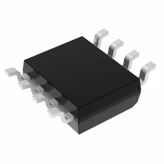
Housed in an 8-pin SOIC with 3.90 mm body width, the CY2305SXC-1T uses a standard, widely supported footprint. No exposed pad, no thermal vias needed — the part dissipates very little power (PLL + CMOS outputs). The shipping options include Tape & Reel and Cut Tape, which covers both prototyping and production volumes.
It is ROHS3 compliant. If the commercial temperature grade is too restrictive, the CY2305SXI-1HT (-40°C to 85°C) is a functional drop-in alternative with the same pinout and performance.