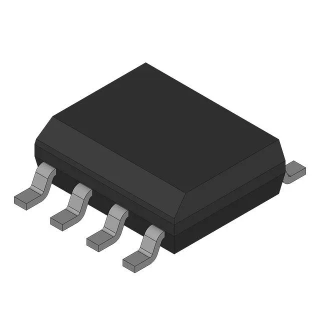
Infineon Technologies CY2304SI-2 — Clock & Timing ICs

Infineon CY2304SI-2 Zero Delay Buffer, 133 MHz, 8-SOIC

MPNCY2304SI-2
End of Life

Infineon Technologies CY2304SI-2 PLL-based zero delay buffer, 133 MHz max, 1:4 input-to-output, 3V-3.6V supply, -40°C to 85°C, 8-SOIC surface mount.

$4.28Ref. price · indicative, final on quote
Packaging8-SOIC (0.154", 3.90mm Width)
RoHSRoHS non-compliant
Independent supplier — new & surplus stockAuthenticity-screened · ESD-safe packingListing updated Aug 2026

Specifications

CY2304SI-2 specifications
ParameterValue
TypeZero Delay Buffer
MountingSurface Mount
Voltage3V ~ 3.6V
Frequency133MHz
Operating temperature-40°C ~ 85°C (TA)
PLLYes
InputClock
OutputClock
PackageBulk
Case8-SOIC (0.154\", 3.90mm Width)
Divider (Multiplier)Yes/No
Number of circuits1
Ratio - Input:Output1:4
Differential - Input:OutputNo/No

Product details

PLL-based zero delay buffer for clock distribution

The Infineon CY2304SI-2 is a PLL-based zero delay buffer designed to regenerate a clock input with deterministic phase alignment, fanning out one clock source to four outputs at up to 133 MHz.

133 MHz fan-out with 1:4 ratio

The 1:4 input-to-output ratio means one clock input drives four output copies, each phase-locked to the reference — useful for distributing a master clock to multiple FPGAs, ASICs, or memory interfaces on the same board. With no differential I/O, the buffer accepts single-ended clock inputs and delivers single-ended outputs, keeping the routing simple on a standard 2- or 4-layer PCB. The divider/multiplier is listed as Yes/No, indicating the device can divide the input frequency but does not multiply it — the output frequency is equal to or a sub-multiple of the input, not a higher multiple.

8-SOIC package and supply integration

The single-circuit design (one PLL core) drives all four outputs from one clock tree, simplifying decoupling — a single 0.1 µF cap near the supply pin per the datasheet recommendation is typical.

Active lifecycle and compliance note

The device is marked RoHS non-compliant — a legacy BOM flag for designs that still permit tin-lead solder processes or require lead-bearing finishes for high-reliability applications.

Frequently asked questions

What is the CY2304SI-2's maximum output frequency?

The maximum frequency is 133 MHz, which sets the ceiling for the clock tree — the four outputs will all run at or below this frequency, depending on the input clock and any divider setting.

Is the CY2304SI-2 RoHS compliant?

No, Infineon lists it as RoHS non-compliant. This means the device may contain lead in the solder finish or other restricted substances — verify your assembly process and regulatory requirements before specifying.