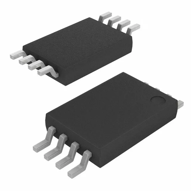
Infineon Technologies CY2304NZZXC-1T — Clock & Timing ICs

CY2304NZZXC-1T Clock Buffer, 140 MHz, 1:4 Fanout, 8-TSSOP

MPNCY2304NZZXC-1T
End of Life

Infineon (Cypress) CY2304NZZXC-1T, Zero-Delay Clock Buffer, 1 Circuit, 1:4 I/O, LVCMOS/LVTTL Input, LVCMOS Output, 140 MHz Max, 3V-3.6V Supply, 0°C-70°C, 8-TSSOP.

$11.39Ref. price · indicative, final on quote
Packaging8-TSSOP (0.173", 4.40mm Width)
StockContact for availability
MOQ1 pcs
  • 100% new & originalTraceable channels only — no refurbs, no pulls, no remarked parts.
  • Date & lot codes on quoteStated per line before you commit; label photos on request.
  • MSL-compliant ESD packingMoisture-sealed bags with indicator cards; reels photo-verified.
  • PayPal buyer protectionPay by T/T, PayPal or Payoneer — card payments covered end to end.

Specifications

CY2304NZZXC-1T Technical Specifications
ParameterValue
Mounting typeSurface Mount
Voltage3V ~ 3.6V
Frequency140MHz
Operating temperature0°C ~ 70°C
PLLNo
InputLVCMOS, LVTTL
OutputLVCMOS
PackageTape & Reel (TR); Cut Tape (CT)
Main purposePCI Express (PCIe)
Case8-TSSOP (0.173\", 4.40mm Width)
Number of circuits1
Ratio - Input:Output1:4
Differential - Input:OutputNo/No

Product details

What this part is — and the selection trap it avoids

The Infineon (Cypress) CY2304NZZXC-1T is a zero-delay clock buffer designed specifically for PCI Express (PCIe) reference clock distribution. It takes one LVCMOS or LVTTL input and fans it out to four LVCMOS outputs, with a maximum operating frequency of 140 MHz. The part has no internal PLL — it is a buffer, not a synthesizer — so the output clock tracks the input frequency and phase exactly, within the device's propagation delay. This matters because a common selection mistake is grabbing a general-purpose PLL-based fanout buffer for a PCIe clock tree, which adds jitter and can violate the PCIe reference clock specification. The CY2304NZZXC-1T avoids that: it is a clean, low-additive-jitter buffer purpose-built for the PCIe reference clock lane.

Supply and temperature — the commercial-grade reality

Operating from a 3 V to 3.6 V supply, this part is a 3.3 V nominal device — the standard PCIe reference clock rail. The operating temperature range is 0°C to 70°C, which is commercial grade. That means it is intended for office-environment equipment, not industrial or automotive applications. If your PCIe clock distribution needs to survive -40°C or +85°C, this is not the part; look at the industrial-temperature variant in the same family.

Package and footprint — what the 8-TSSOP means for the board

Housed in an 8-TSSOP package (4.40 mm width, 0.173" body width), this is a surface-mount part. The 8-pin TSSOP is a common footprint, and the supplier device package is also listed as 8-TSSOP, so there is no ambiguity about the land pattern. The part is available in Tape & Reel or Cut Tape, which covers both production reels and prototype quantities. No exposed thermal pad here — the 8-TSSOP dissipates through the leads and the board copper, so for high-frequency PCIe clock distribution at 140 MHz, the power dissipation is low enough that thermal management is not a concern.

Lifecycle and compliance — active, no obsolescence worry

There is no NRND or EOL flag on this part. It is also ROHS3 compliant, so it meets the latest EU RoHS exemption-free requirements. For a BOM line that needs a stable, long-life PCIe clock buffer, this part is not a sourcing risk.

Frequently asked questions

What is the maximum frequency of CY2304NZZXC-1T?

The maximum operating frequency is 140 MHz. This is the upper limit for the PCIe reference clock it is designed to buffer and distribute.

Is CY2304NZZXC-1T RoHS compliant?

Yes, it is ROHS3 compliant, meeting the latest EU RoHS directive without exemptions.