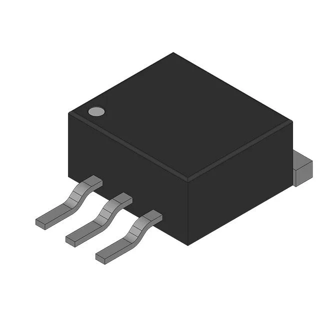
What the DPAK package and P-channel polarity mean on the bench
The AUIRFR5505TRL: The DPAK footprint is a common power-semiconductor package that demands a copper pad on the PCB for thermal dissipation — the 57 W power rating assumes that pad is present and sized per the datasheet layout. P-channel means the load connects between drain and ground, and the gate is pulled low to turn the FET on — useful for high-side switching where you want to avoid a charge-pump gate driver.
On-resistance and the switching current that matters
The maximum on-resistance is 110 mOhm at Vgs = -10 V and Id = 9.6 A — that is the operating point the datasheet guarantees, not the 18 A peak. At 18 A the die will be dissipating well over 35 W even at the Rds(on) floor, so the 57 W package limit means the duty cycle and heatsinking must be checked against the actual load current. Gate charge is 32 nC at Vgs = -10 V — a typical gate driver with 1 A peak output can switch this FET in under 50 ns, but the total switching loss depends on the gate-drive loop inductance as much as the Qg.
Temperature range and where this part survives
Junction temperature range is -55 °C to 150 °C, which covers automotive under-hood and industrial motor-drive environments — the threshold voltage shifts with temperature, so the 4 V max at 250 µA is the cold-start worst case. The gate-source voltage is limited to ±20 V absolute maximum — a gate driver with a 12 V supply is safe, but any ringing above that on the gate node will punch through the oxide.