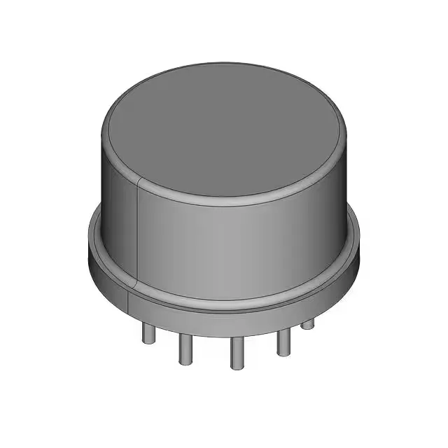
40 V N-channel in the DIRECTFET M2 can
The AUIRF7734M2TR: The DIRECTFET M2 package is a surface-mount can with a solderable top-side source clip and bottom-side drain pad — the dual-sided thermal path pulls heat into the PCB copper plane and, with the right layout, into an external heatsink on the top. The 2.5 W power dissipation figure is the package-limited rating; actual capability depends on the board's thermal stack-up and airflow.
Gate drive and switching parametrics
Gate-source voltage is rated ±20 V, giving margin for a 10 V or 12 V gate drive rail. The typical gate charge is 72 nC at 10 V — a gate driver delivering 2 A peak can switch the FET in under 40 ns, which matters for hard-switching topologies where crossover losses scale with transition time. The 0.0025 µF (2.5 nF) input capacitance is the sum of Ciss at the test condition; it sets the gate-drive power budget. At 500 kHz switching frequency, the gate-drive loss is roughly Qg × Vgs × fsw, or about 0.36 W — within the driver's thermal budget but worth derating if the ambient exceeds 85 °C. Threshold voltage is 4 V maximum at 100 µA drain current.
The 175 °C Tj(max) is the silicon limit; the package and solder joint reliability at that temperature depend on the PCB material (high-Tg FR-4 or polyimide) and the thermal cycling profile.