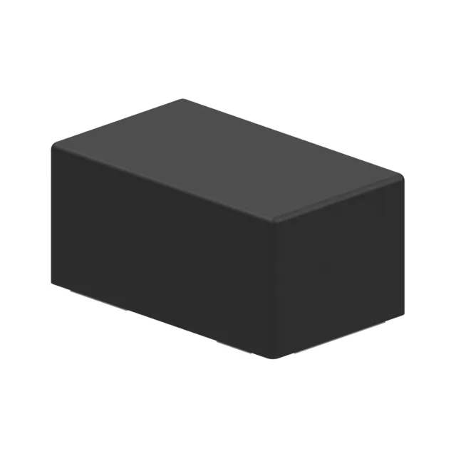
Bidirectional Zener clamp for 5V signal lines
The D5V0P1B2LP-7B: Its 5.5V (Max) reverse standoff voltage sits just above a nominal 5V supply, so the device stays transparent during normal operation and only conducts when a transient pushes the line above the 6V minimum breakdown threshold. With a clamping voltage of 13V at a peak pulse current of 4A (8/20µs waveform), this part limits the voltage seen by the downstream IC to 13V during a 4A surge — enough to protect a 5V-tolerant GPIO or power input from ESD or short-duration overvoltage events. The 8pF capacitance at 1MHz keeps signal integrity intact on high-speed data lines up to the low-MHz range.
X1-DFN1006-2 footprint and board integration
Housed in the X1-DFN1006-2 package (the DFN variant of the 0402 / 1006 Metric footprint), this TVS measures 1.0 mm × 0.6 mm with a seated height under 0.5 mm — it fits under a low-profile shield or alongside a dense BGA. The two-pad layout routes the signal through one pad and the ground plane through the other; the short trace between the TVS and the protected IC is critical to keep the clamping loop inductance low. Surface-mount assembly on standard FR-4 with a 0402 solder paste aperture is straightforward. The -65°C to 150°C junction temperature range covers automotive under-hood and industrial ambient extremes, though the part carries no explicit AEC-Q grade in the listing.
Active production — sourcing posture
The base product number D5V0P1 covers the family; the -7B suffix denotes the X1-DFN1006-2 package and tape-and-reel packaging.