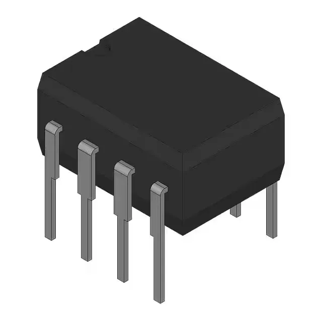
Analog Devices TSC428EJA

TSC428EJA Dual MOSFET Driver, 1.5A Peak, 8-CDIP

MPNTSC428EJA
End of Life

TelCom Semiconductor TSC428EJA dual low-side MOSFET driver, 1.5A peak output, 20ns typ rise/fall, 4.5V to 18V supply, inverting and non-inverting inputs, 8-CDIP (0.300", 7.62mm) through-hole ceramic package.

$1.07Ref. price · indicative, final on quote
Packaging8-CDIP (0.300", 7.62mm)
StockContact for availability
MOQ1 pcs
  • 100% new & originalTraceable channels only — no refurbs, no pulls, no remarked parts.
  • Date & lot codes on quoteStated per line before you commit; label photos on request.
  • MSL-compliant ESD packingMoisture-sealed bags with indicator cards; reels photo-verified.
  • PayPal buyer protectionPay by T/T, PayPal or Payoneer — card payments covered end to end.

Specifications

TSC428EJA Technical Specifications
ParameterValue
Gate typeN-Channel, P-Channel MOSFET
Input typeInverting, Non-Inverting
Channel typeIndependent
Mounting typeThrough Hole
Voltage4.5V ~ 18V
Logic voltage - VIL, VIH0.8V, 2.4V
Current - peak output (Source, sink)1.5A, 1.5A
PackageBulk
Case8-CDIP (0.300\", 7.62mm)
Number of drivers2
Driven configurationLow-Side
Rise (Fall time)20ns, 20ns

Product details

Dual 1.5A low-side driver in a hermetic ceramic DIP

The TelCom Semiconductor TSC428EJA is a dual-channel, low-side MOSFET driver capable of sourcing and sinking 1.5A peak current per channel, with a typical rise and fall time of 20ns. It operates from a 4.5V to 18V supply rail, making it compatible with 5V logic as well as 12V or 15V industrial gate-drive buses. The independent inverting and non-inverting inputs give you polarity flexibility per channel — handy when one MOSFET needs a high-side bootstrap and the other a direct low-side drive.

The 20ns rise/fall time reduces MOSFET switching losses by minimizing time in the linear region.

Ceramic DIP — built for harsh environments

The 8-CDIP (0.300", 7.62mm) ceramic package with through-hole mounting is a deliberate choice for applications where plastic packages won't hold up — think avionics, downhole tools, satellite power supplies, or military-grade power converters. The hermetic seal keeps moisture and contaminants out, and the ceramic body handles wider temperature swings without cracking.

Supply range and logic thresholds

The 4.5V to 18V supply range covers the common gate-drive voltages for both logic-level and standard MOSFETs. The logic input thresholds are specified at 0.8V (VIL) and 2.4V (VIH), so the inputs are directly compatible with 3.3V and 5V logic families without external level shifting. At 5V supply, a 3.3V microcontroller output will reliably drive the inputs high; at 12V supply, the 2.4V VIH still leaves margin for 5V logic.

Frequently asked questions

What is the pinout of TSC428EJA?

Design engineers need to confirm pin compatibility before PCB layout.

Is TSC428EJA in stock?

Sourcing buyers need immediate availability to avoid production delays.

What is the price of TSC428EJA?

Buyers compare cost to budget and negotiate with distributors.

What are alternatives to TSC428EJA?

Engineers and buyers seek drop-in replacements for supply chain flexibility.

Is TSC428EJA obsolete?

Brokers and maintenance techs need lifecycle status to plan long-term support.

What is the supply voltage range of TSC428EJA?

Ensures the driver works with the existing power rail without redesign.