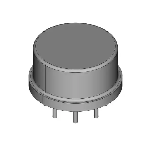
Dual JFET op-amp in hermetic TO-99-8 — military temperature range
The OP215BJ/883C is a dual JFET-input operational amplifier from the 883C screening class, supplied in a hermetic TO-99-8 metal can package. Typical applications include precision analog signal conditioning, active filtering, and data acquisition in avionics, satellite, and defense systems where hermetic sealing and extended temperature rating are required.
Slew rate and bandwidth — what they mean for signal chain design
The 18 V/µs slew rate supports large-signal output swings up to several hundred kilohertz without significant distortion, making the part suitable for fast-settling analog front ends and waveform generation. The 5.7 MHz gain-bandwidth product sets the small-signal closed-loop bandwidth; for a gain of 10, the usable bandwidth is approximately 570 kHz. These parameters are adequate for many sensor-conditioning and control-loop applications, though designers targeting higher-speed data converters or video bandwidth should evaluate the 16 MHz AD823ARZ-RL as an alternative.
JFET input stage — picoamp bias current for high-impedance sources
The JFET input stage provides an input bias current of 15 pA, which is critical when interfacing with high-impedance sensors such as photodiodes, piezoelectric transducers, or high-value resistive dividers. The 800 µV input offset voltage is moderate; for precision dc applications requiring sub-100 µV offset, the AD712KNZ (300 µV) may be a better fit, though it lacks the military temperature range.
Package and mounting — through-hole hermetic metal can
The TO-99-8 metal can package is a through-hole, hermetically sealed enclosure designed for high-reliability environments. It is compatible with standard 8-pin round sockets or direct solder to a PCB. The metal can provides inherent shielding against electromagnetic interference and is required for many military and space screening flows.
Lifecycle and compliance — active, RoHS non-compliant
It is RoHS non-compliant, which is typical for hermetic military-grade components and acceptable under most defense and aerospace procurement exemptions.