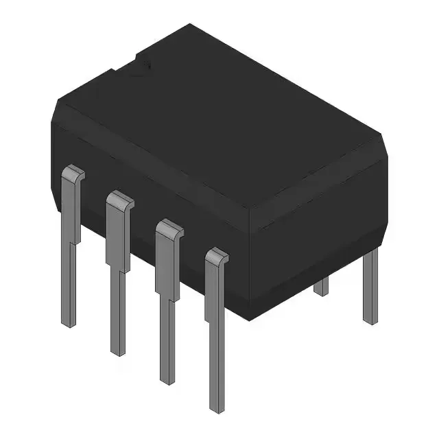
JFET op-amp for ±15 V industrial signal chains
It delivers 5.4 MHz gain-bandwidth product and 9 V/µs slew rate, with a typical input bias current of 60 pA and maximum input offset voltage of 500 µV.
The 60 pA input bias current is low enough for high-impedance sensor interfaces (photodiodes, pH probes) where a bipolar op-amp's µA-level bias would create offset errors. The 500 µV input offset is adequate for general-purpose 12-bit signal chains but not precision DC measurement; if you need sub-100 µV offset, look at the AD8510 family instead. Supply range of 36 V (max) allows operation on standard ±15 V industrial rails with 6 V of headroom — useful for motor-drive feedback or PLC analog I/O modules where the supply is already regulated. Quiescent current of 2.8 mA is moderate; in a multi-channel board with ten of these, the total supply draw hits 28 mA, which a typical 78xx regulator handles without issue.
The part is RoHS non-compliant, using a tin-lead (SnPb) finish. If your assembly line is RoHS-only and exempted for leaded solder under a military or medical exemption, this part fits; otherwise you will need a Pb-free alternate such as the AD8627AKSZ-REEL7 (surface-mount, RoHS compliant) or a through-hole JFET op-amp from the OP15 family that is listed as RoHS compliant.
Package and form factor
Supplied in 8-pin DIP (0.300" width, 7.62 mm pitch) — standard through-hole footprint for breadboard prototyping, socketed test boards, or retrofit into legacy PCB designs that cannot migrate to surface-mount.