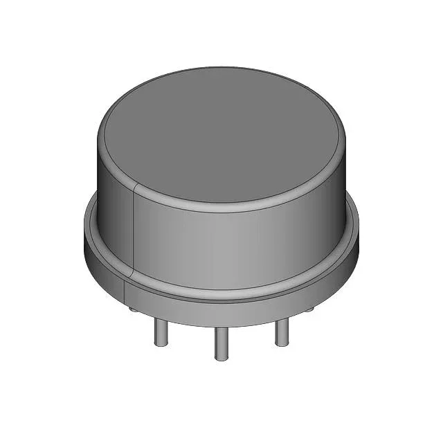
Precision instrumentation amplifier in a hermetic TO-99 can
The OP05BICJ is a single-circuit instrumentation amplifier from the OP05 series, packaged in a TO-99-8 metal can for through-hole mounting. It is designed for precision analog signal conditioning where low offset and bias current are required over a wide temperature range. Key characteristics include a 0.3 V/µs slew rate, 200 µV input offset voltage, and 1 nA input bias current, operating from a 6 V to 36 V supply span.
The 0.3 V/µs slew rate limits the large-signal bandwidth to approximately 4.8 kHz at 10 V output swing. This is adequate for strain-gauge bridges, thermocouple amplifiers, and other low-frequency sensor interfaces where noise rejection and DC accuracy matter more than speed. For applications requiring faster settling, a higher-slew-rate instrumentation amplifier such as the AD623 (0.3 V/µs in surface-mount) would be a functional alternative, though the OP05BICJ's TO-99 package and military temperature range are not matched by that part.
200 µV input offset and 1 nA bias — DC accuracy for bridge and thermocouple circuits
The 200 µV maximum input offset voltage sets the error floor before external gain. With a gain of 100, this offset appears as 20 mV at the output, which must be nulled or calibrated out in precision measurement chains. The 1 nA input bias current is low enough for high-impedance sources such as pH probes or piezoelectric sensors, but not as low as CMOS-input instrumentation amplifiers (typically picoamps). For source impedances above 100 kΩ, the bias current multiplied by source resistance adds a voltage error that should be budgeted.
TO-99-8 metal can — hermetic package for high-reliability programs
The TO-99-8 metal can provides a hermetic seal against moisture and contaminants, making it suitable for military, aerospace, and downhole applications where plastic packages are not accepted. The through-hole mounting requires a drilled PCB and manual or wave-solder assembly; no surface-mount reflow profile applies. The metal case also offers improved thermal dissipation compared to plastic DIP packages, though the junction-to-ambient thermal resistance is still dominated by the leads.
Active lifecycle, RoHS non-compliant — sourcing for long-life programs
This simplifies procurement for multi-year programs that require a stable, qualified part. However, the device is RoHS non-compliant due to lead (Pb) in the solder terminations. For EU-regulated assemblies, an exemption (e.g., RoHS Annex III, category 8 or 9 for industrial monitoring and control) must be documented.