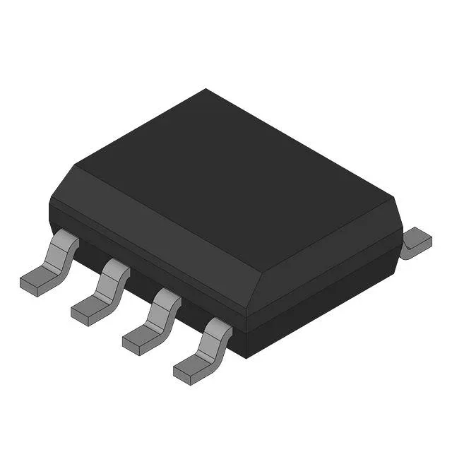
Analog Devices MAX9381ESA — Logic ICs

MAX9381ESA D-Type Flip-Flop, 3 GHz, -2.25V to -5.5V, SOIC-8

MPNMAX9381ESA
End of Life

Analog Devices MAX9381ESA D-Type Flip-Flop, 3 GHz clock frequency, -2.25V to -5.5V supply, negative-edge triggered, complementary outputs, 8-SOIC package, industrial temperature range.

$5.82Ref. price · indicative, final on quote
Packaging8-SOIC (0.154", 3.90mm Width)
StockContact for availability
Lead timeIn Stock wk
MOQ1 pcs
  • 100% new & originalTraceable channels only — no refurbs, no pulls, no remarked parts.
  • Date & lot codes on quoteStated per line before you commit; label photos on request.
  • MSL-compliant ESD packingMoisture-sealed bags with indicator cards; reels photo-verified.
  • PayPal buyer protectionPay by T/T, PayPal or Payoneer — card payments covered end to end.

Specifications

MAX9381ESA Technical Specifications
ParameterValue
TypeD-Type
Output typeComplementary
Trigger typeNegative Edge
Mounting typeSurface Mount
Voltage-2.25V ~ -5.5V
Frequency3 GHz
Operating temperature-40°C ~ 85°C (TA)
PackageBulk
FunctionStandard
Case8-SOIC (0.154\", 3.90mm Width)
Number of elements1
Number of bits per element1

Product details

3 GHz clock and negative supply — the fit decision

The MAX9381ESA: This D-type flip-flop clocks at 3 GHz, making it suitable for high-speed data retiming, clock recovery, and serializer-deserializer (SerDes) applications where a standard 100-200 MHz logic part cannot hold the edge rate. The part operates on a negative rail relative to ground, which is typical for ECL (Emitter-Coupled Logic) families but unusual for TTL or CMOS systems. Confirm that your board's power tree includes a negative voltage regulator before specifying this part. Negative-edge trigger means the output changes state on the falling edge of the clock signal. This complements positive-edge-triggered parts in the same data path and is a deliberate selection for clock-phase alignment.

Industrial temperature and SOIC-8 package integration

No special fan-out or via-in-pad is required for a two-layer board at these speeds, though the 3 GHz clock edge may need controlled-impedance traces on the clock input.