Quiescent current is 400 µA max. Input offset voltage is 7 mV max at 5V.
Output drive and input bias
Input bias current maxes at 0.25 µA at 5V, so high-impedance sources like thermistors or photodiodes won't see significant loading error. The 100 ns propagation delay includes the rise and fall through the open-drain stage — factor in an external pull-up resistor value when budgeting total loop delay for fast fault detection.
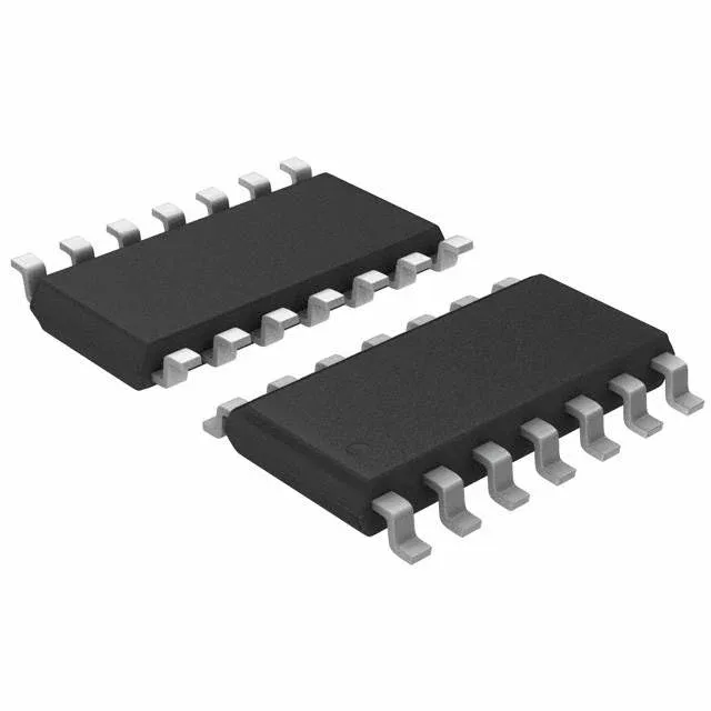
Housed in a 14-SOIC (0.154", 3.90 mm width) surface-mount package. RoHS3 compliant.
ROHS3 compliant, so no exemption expiry risk for EU or UKCA markets. No LTB window to watch — this part is safe for new designs and production BOMs.