Analog Devices MAX9039BEBT+T — Analog & Data Acquisition

MAX9039BEBT+T Comparator with Voltage Reference, 450ns

MPNMAX9039BEBT+T
End of Life

Maxim Integrated MAX9039BEBT+T, single comparator with integrated voltage reference, ±3mV hysteresis, 450ns propagation delay, 2.5V to 5.5V supply, CMOS/TTL outputs, 6-WLP package, -40°C to 85°C.

$2.03Ref. price · indicative, final on quote
Packaging6-WFBGA, WLBGA
RoHSROHS3 Compliant
Sourced new & surplus through independent channelsAuthenticity-screened · ESD-safe packingListing updated Aug 2026

Specifications

MAX9039BEBT+T specifications
ParameterValue
Typewith Voltage Reference
Output typeCMOS, Push-Pull, Rail-to-Rail, TTL
MountingSurface Mount
Voltage - input offset1mV @ 5V
Voltage - supply, single (Dual (±))2.5V ~ 5.5V
Output current8mA
Current - quiescent100µA
Current - input bias1pA @ 5V
Operating temperature-40°C ~ 85°C
PackageTape & Reel (TR); Cut Tape (CT)
Hysteresis±3mV
Case6-WFBGA, WLBGA
CMRR, PSRR80dB CMRR, 80dB PSRR
Number of elements1
Propagation delay450ns

Product details

Single comparator with a voltage reference on-chip

The Maxim Integrated MAX9039BEBT+T is a single comparator that integrates a voltage reference, saving the external reference resistor divider or reference IC that a standalone comparator would need. It delivers CMOS, push-pull, rail-to-rail, or TTL output drive, and the ±3mV hysteresis cleans up switching around the threshold — handy for sensor threshold detection or battery monitoring where you want a clean digital edge without extra passives.

Propagation delay and quiescent current

Propagation delay is 450ns maximum — moderate speed that works for most level-detection, over-voltage/under-voltage lockout, and window-comparator loops. It is not a high-speed PWM or zero-crossing detector part; if you need sub-100ns response, look elsewhere. Quiescent current maxes at 100µA, so it fits battery-operated gear where every microamp counts. The 8mA output drive is enough to light an LED or drive a logic gate input directly.

Input offset voltage is 1mV max at 5V, and input bias current is 1pA max, so high-impedance sources like pH probes or photodiode amplifiers are manageable.

Package and handling for the 6-WLP

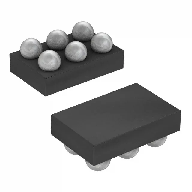
The part comes in a 6-WLP (wafer-level package) — essentially the bare die with solder bumps, no plastic overmold. That means the package is the die itself, so handling requires ESD precautions and a clean, moisture-controlled environment. It is surface-mount only, and the 6-WLP footprint is tiny; rework needs a hot-air station with a fine nozzle and a steady hand. No lab, no bench — but if you have the kit, it is doable. The supplier device package is 6-WLP, and the case code is 6-WFBGA, WLBGA.

Frequently asked questions

What is the propagation delay of MAX9039BEBT+T?

The maximum propagation delay is 450ns. That is moderate speed — fine for threshold detection and monitoring loops, but not for high-frequency switching or fast comparator applications.

Does MAX9039BEBT+T include a voltage reference?

Yes, it integrates a voltage reference on-chip. That is the key feature — it saves an external reference resistor divider or reference IC, simplifying the BOM and board layout.

What package does MAX9039BEBT+T come in?

It comes in a 6-WLP (wafer-level package), also described as 6-WFBGA or WLBGA. It is a tiny, bare-die package with solder bumps — surface-mount only, needs careful handling and hot-air rework.