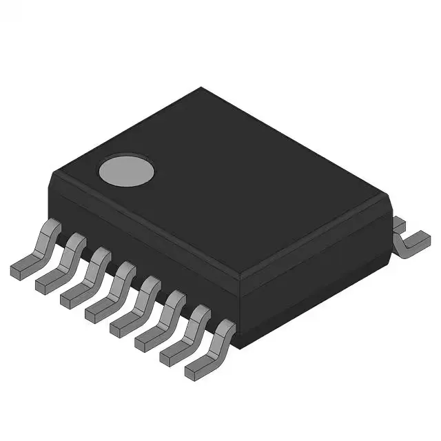
Boost controller for multi-rail portable designs
The MAX863EEE+ is a step-up (boost) DC-DC controller IC from Analog Devices, designed to drive external N-channel MOSFETs for generating regulated positive output voltages above the input rail. It operates from a 1.5V to 11V supply range, making it suited for battery-powered systems where the input voltage drops as cells discharge. The controller provides two transistor-driver outputs, enabling dual-rail generation or interleaved single-rail designs for higher output current.
Package, temperature, and compliance
The tube packaging is the standard delivery format for this order code.
Control features and integration notes
An enable pin allows the controller to be shut down for power savings, while a low-battery comparator provides an early warning flag to the system microcontroller before the input rail collapses. The controller does not integrate synchronous rectification or clock synchronization — the external MOSFET and diode selection determine the efficiency and switching noise profile. For a typical boost application, the reference design in the datasheet shows the external component selection around the 16-QSOP footprint; the layout should keep the high-current loop from the input capacitor through the inductor, MOSFET, and output diode as tight as possible.