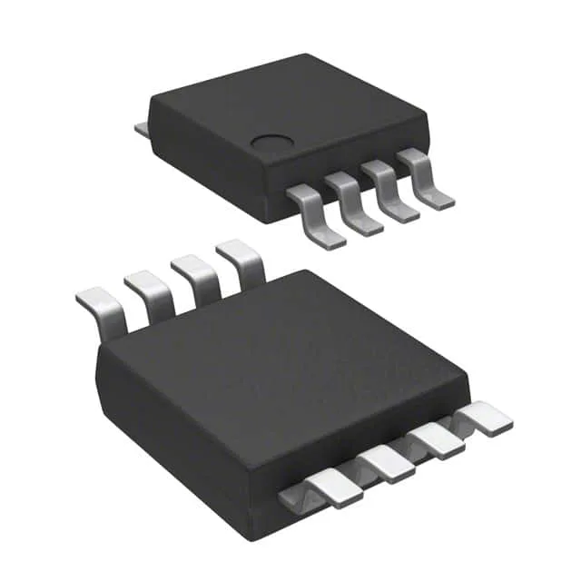
Dual 8-bit DAC in a small serial package
The MAX549ACUA+ is a dual 8-bit, voltage-output digital-to-analog converter from Maxim Integrated, built around an R-2R ladder architecture. It packs two independent DACs into an 8-pin 8-uMAX/uSOP package — about 3×3 mm — so it fits on tight mixed-signal boards where a separate reference and output buffer would eat real estate. The SPI data interface keeps the pin count low: three wires (SCLK, DIN, CS) plus the output and supply rails. Settling time is 4 µs typical, which means the output reaches within ½ LSB of the final value in that window — fast enough for a control-loop update running at a few tens of kilohertz, or for trimming a bias voltage during power-on calibration.
Supply rails and output drive
That simplifies the power tree: one LDO or a clean 3.3 V bus feeds the whole part. The output is voltage-unbuffered, so the DAC's output impedance is the R-2R ladder resistance (typically 10 kΩ). It drives a high-impedance load directly, but for a 50 Ω or 100 Ω input, add an external op-amp buffer. The reference input is external, so the full-scale output voltage equals the reference voltage times the digital code divided by 256. An external 2.5 V reference gives a 0 V to 2.5 V output span; a 4.096 V reference gives a 0 V to 4.096 V span. The INL/DNL spec is -, ±0.9 LSB max — the DNL is guaranteed monotonic, meaning the output always increases for increasing digital codes, which matters in closed-loop control where a non-monotonic step would reverse the feedback sign.
Temperature grade and board-fit
That covers most benchtop instruments, industrial control cabinets with HVAC, and consumer electronics. For an engine bay or outdoor enclosure that sees -20°C, look at the industrial-temperature variant in the same family. The 8-TSSOP/8-MSOP footprint (0.118-inch body width, 3.00 mm) is a standard JEDEC outline. The 8-uMAX/uSOP supplier package is Maxim's own naming for the same 3×3 mm MSOP-8. No exposed pad; thermal dissipation is through the leads only.