Octal 12-bit DAC with buffered voltage outputs
The MAX5307EUE-TG077 is an octal 12-bit digital-to-analog converter from Analog Devices, delivering eight independent voltage outputs from a single 16-TSSOP package. Each DAC channel settles to within 1/2 LSB in 5 µs typical, which means the part can update all eight outputs in under 40 µs — fast enough for closed-loop control loops and multi-channel trim applications running at update rates above 20 kHz. The output is voltage-buffered, so each channel can drive a moderate load directly without an external op-amp, though the buffer's output impedance and capacitive-load stability should be checked against the specific load in the BOM.
SPI/DSP interface and supply rails
Data is written via a 3-wire SPI-compatible serial interface that also supports DSP frame-sync protocols — a single daisy-chain line serves all eight channels, keeping the digital fan-out on the host controller to one chip-select and one serial clock. If separate rails are used, the digital supply can be as low as 2.7 V while the analog section runs at 5 V, which keeps the output swing near the top rail. The reference input is external — the output span is set by the voltage applied to the REF pin. A 2.5 V reference gives a 0 V to 2.5 V output range; a 5 V reference gives a 0 V to 5 V range. The INL is specified at ±1 LSB maximum, which at 12 bits and a 5 V reference is a 1.22 mV endpoint error.
Package and temperature grade
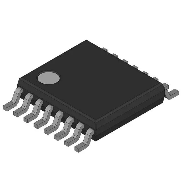
Housed in a 16-lead TSSOP with a 4.40 mm body width and 0.65 mm pin pitch, the MAX5307EUE-TG077 fits on a standard 2-layer PCB without micro-vias. The surface-mount package is suited for reflow assembly.