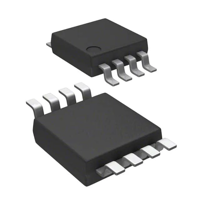
The MAX5302CUA+ is a 12-bit, voltage-buffered DAC from Maxim Integrated, built on an R-2R ladder architecture. It converts a serial SPI word into an analog output voltage with a 14 µs typical settling time to ±0.5 LSB. The reference is external, so the absolute output accuracy and temperature drift are determined by the reference voltage source you pair with it — not by an internal bandgap. This gives you control over the system accuracy budget but also means the reference's noise and drift directly appear at the output.
Accuracy budget: INL, DNL, and monotonicity
Integral non-linearity is ±4 LSB maximum, which at 5 V reference and 12 bits (1.22 mV per LSB) means the output can deviate from the ideal transfer by up to 4.88 mV at any code. That is the error budget a calibration technician would account for in a production test limit. Differential non-linearity is ±1 LSB maximum, guaranteeing monotonicity — every increase in digital code produces a positive or zero voltage step, never a negative step. This is critical for closed-loop control where a non-monotonic DAC would cause the loop to reverse direction momentarily. The R-2R architecture inherently provides low glitch energy at major-code transitions compared to segmented architectures, which matters when the DAC drives a sample-and-hold or a modulator that is sensitive to transient spikes.
Settling time and update rate — what 14 µs means for your loop
The 14 µs typical settling time to ±0.5 LSB sets the maximum update rate at roughly 71 kHz for a full-scale step. For a control loop running at 10 kHz, the DAC settles in about one-seventh of the sample period, leaving margin for the ADC conversion and the control algorithm. The SPI interface runs at standard clock rates — the settling time, not the serial clock, is the throughput bottleneck. A 10 MHz SPI clock loads a 16-bit word (12 data + control bits) in 1.6 µs, after which the DAC needs the full 14 µs to settle before the next conversion starts.
Package, temperature grade, and board integration
The supplier device package is 8-uMAX/uSOP, which is the standard Maxim thin MSOP variant. Mounting is surface-mount only; the tube packaging is suitable for prototype builds and low-volume production but not for automated tape-and-reel feeders without manual loading.
Active lifecycle and compliance status
Because the part is active and the reference is external, the only long-term drift concern is the external reference component — the DAC itself has no aging mechanism that affects the transfer function beyond the initial INL/DNL tolerance.