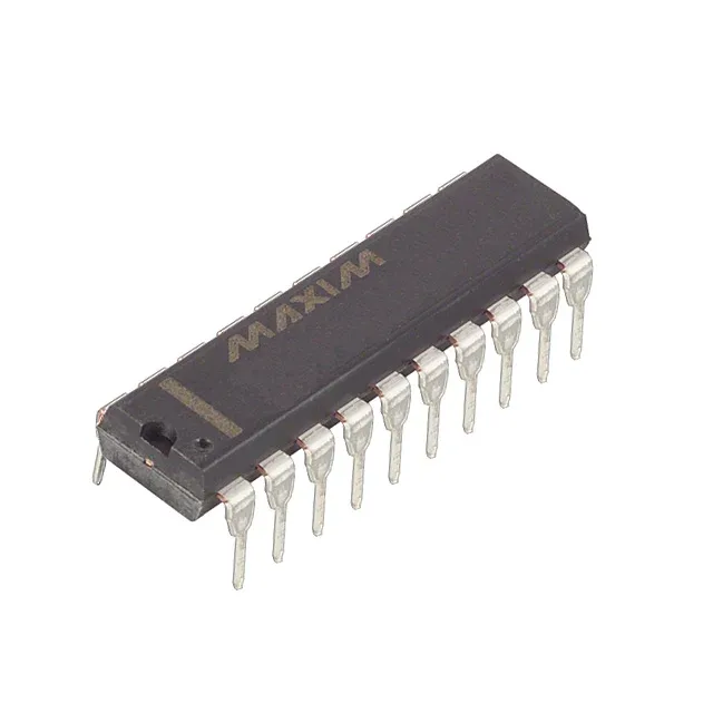
8-bit quad DAC in a 20-pin PDIP — the board-fit story
The MAX509BCPP+ is an 8-bit digital-to-analog converter with four independent voltage-buffered outputs, each settling to ½ LSB in 6 µs typical. The 20-pin PDIP (0.300" wide, 7.62 mm) is a through-hole package that fits standard DIP sockets or solder-in on a 0.100" pitch prototype board — no fine-pitch stencil needed, and the 100-mil lead spacing is hand-solderable in a rework loop. Four DACs in one package means a single SPI bus (data interface is SPI) and one external reference serve all four channels. The analog supply is ±5 V, the digital supply is 5 V — the split rails let the output swing near the analog rails while the digital core stays at a single 5 V level.
R-2R architecture and what the linearity spec means
The R-2R ladder architecture uses matched resistor ratios rather than a switched-capacitor charge-redistribution network — the INL spec is not explicitly stated, but the DNL is ±1 LSB max. A ±1 LSB DNL means no missing codes at 8-bit resolution; every digital input produces a unique analog output, and the step size between adjacent codes stays within one LSB of ideal. For an 8-bit DAC with 256 steps, a DNL within ±1 LSB guarantees monotonicity — the output always increases as the digital code increments. The 6 µs settling time is measured to ½ LSB for a full-scale step — this sets the per-channel update rate ceiling. With four channels, the SPI clock must complete a 16-bit frame (8-bit data plus control bits) within the settling window to avoid output contention. At 6 µs per channel, the aggregate throughput is roughly 166 kSPS across all four DACs if the SPI bus runs at 10 MHz or faster.
Active lifecycle and compliance documentation
The part is supplied in Tube packaging, the standard 20-PDIP tube quantity.