Switch topology and signal path fit
The MAX4702ETE+ packs four independent SPDT switches in a 2:1 multiplexer/demultiplexer configuration per circuit (cites:,). Each switch routes one of two inputs to a common output, or the reverse — useful for signal routing, gain selection, or multiplexing multiple sensor channels into a single ADC input. The 250 MHz -3 dB bandwidth (cites:) and -79 dB crosstalk at 1 MHz (cites:) mean this switch passes high-frequency signals like video or IF with minimal bleed between channels. For a 4-channel video multiplexer or a software-defined radio front-end, the isolation spec keeps adjacent channels from coupling into the active path.
Supply rail and switching performance
The 35 ns turn-on and 20 ns turn-off times (cites:) support fast channel scanning in data acquisition systems where the multiplexer must settle before the ADC samples. On-resistance is 75 ohm maximum (cites:) with 2 ohm channel-to-channel matching (cites:). For a precision analog front-end, the matching figure keeps the gain error consistent across all four channels — the 2 ohm delta at 75 ohm nominal is about 2.7% mismatch, which is acceptable for 10-bit systems but may need calibration at 12+ bits.
Charge injection and leakage for precision circuits
Charge injection is 0.5 pC typical (cites:) — when the switch turns off, the injected charge creates a voltage glitch on the hold capacitor in a sample-and-hold circuit. For a 10 pF hold cap, 0.5 pC produces a 50 mV step; the downstream ADC must settle past this before the conversion completes. The 500 pA max off-leakage (cites:) keeps the droop rate low during the hold interval.
Package and thermal interface
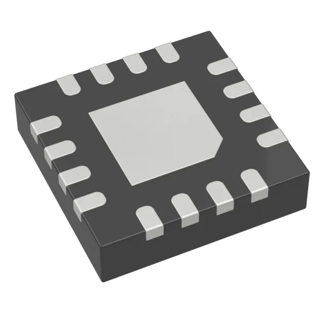
The 16-WFQFN with exposed pad (cites:) measures 3x3 mm in the 16-TQFN supplier package (cites:). The 0.5 mm pitch QFN demands a solder-paste stencil with 0.25 mm apertures and a reflow profile peaking at 260 °C peak for lead-free assembly.
