What the -92 dB crosstalk actually means for your signal chain
The MAX399EGE is a precision dual 4:1 multiplexer (two independent SP4T switches) from Analog Devices' MAX399 family. Its -92 dB crosstalk at 100 kHz means that when you are switching a 1 Vpp signal on channel 1, less than 250 µV of that signal bleeds into channel 2 at the same frequency. For a 16-bit ADC with a 5 V reference, that is well below 1 LSB of interference — the mux does not limit your system's noise floor in most precision analog front-ends. The 100 Ohm max on-resistance tells you the series resistance the signal sees when the channel is closed. Driving a 10 kOhm load, the voltage error from Ron is about 1%. For a 1 kOhm load, it is a 10% divider — you need a buffer amplifier after the mux for low-impedance loads. The 6 Ohm channel-to-channel matching means the Ron difference between any two channels is at most 6 Ohms, which keeps gain errors consistent across channels in a multiplexed system.
Supply flexibility — single or dual rails
The total supply span is the same either way — 6 V to 16 V. With dual rails, the analog signal can swing symmetrically around ground, which is useful for bipolar sensor signals like thermocouple outputs or strain-gauge bridges. On a single rail, the signal must be biased above ground to stay within the common-mode range. The 150 ns max switch time (both Ton and Toff) means the mux settles fast enough for audio-frequency scanning and low-speed data acquisition. At 1 MHz switching, the 150 ns transition is 15% of the period — fine for muxing before a SAR ADC that samples at 100 kSPS. Not fast enough for video or RF switching, where sub-10 ns parts are needed.
Package and temperature — board-fit reality
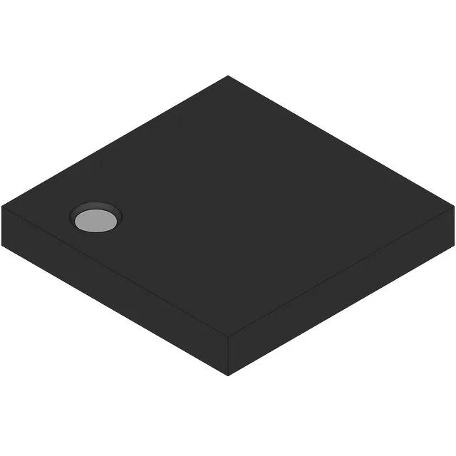
The MAX399EGE comes in a 16-VQFN with exposed pad, 4 mm x 4 mm body (supplier device package 16-QFN). The part is rated for the full range, so no derating needed for factory-floor enclosures or outdoor telecom cabinets. Not qualified for under-hood automotive (that would need -40°C to +125°C and AEC-Q100).
Active production — sourcing posture
The package is listed as Bulk delivery — this is the shipping format (tubes or trays), not a package type. The actual IC package is the 16-VQFN Exposed Pad described above. Bulk packaging is typical for engineering samples and low-volume production runs; for high-volume tape-and-reel, check the -TR suffix variant if available.