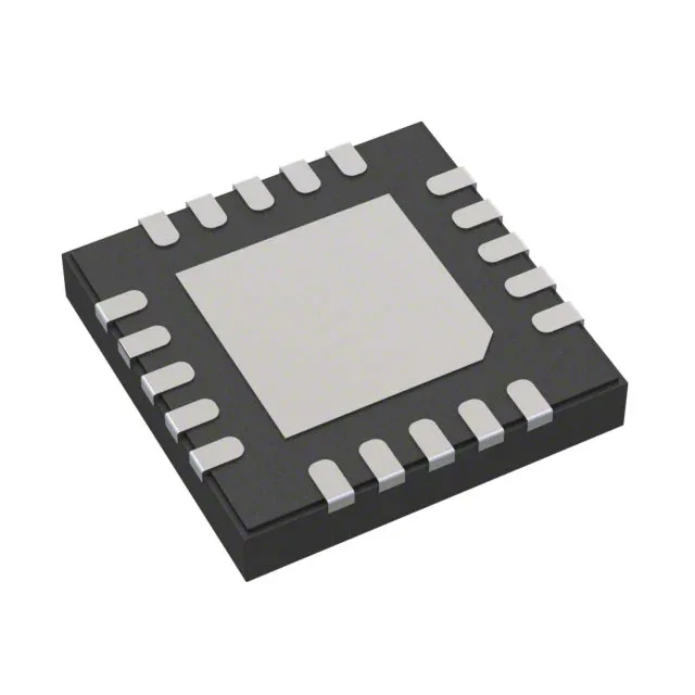
Board-fit and package integration
The MAX25206ATPA/VY+ comes in a 20-lead SWTQFN (4x4 mm) with an exposed pad and wettable flank terminals. The wettable flank geometry allows the solder fillet to climb the side of the package, making the joint visible to an automated optical inspection (AOI) system — a production-line advantage over conventional QFN packages where the solder joint is hidden under the body. The exposed pad under the package must be soldered to a thermal land on the PCB with adequate thermal vias to the ground plane. The junction-to-ambient thermal resistance depends on the copper area on the board; for a 4x4 mm pad, a 1-square-inch copper pour on the top layer is a typical starting point.
Input range and switching — sizing the power stage
The 3.5 V to 60 V input range covers 12 V and 24 V automotive systems with margin for cold-crank dips and load-dump transients. The 60 V absolute maximum on the supply pin means no external clamp is needed for a 48 V load-dump event on a 12 V bus — the controller survives the surge directly. The high frequency also moves the fundamental switching noise above the AM broadcast band, which simplifies filtering in automotive infotainment applications. Synchronous rectification replaces the freewheeling diode with a low-Rds(on) internal FET, raising efficiency by 3-5% at full load compared to a diode-based buck. The synchronous FET also allows the output to sink current during load transients, reducing output overshoot.
Thermal and duty-cycle limits
The 97% maximum duty cycle means the controller can regulate a 3.3 V output from a 3.5 V input — useful for post-regulation after a long cable drop or in battery-powered systems running near end-of-discharge.
Control and synchronization
Current-mode control with cycle-by-cycle current limit protects the external MOSFET and the output from overloads. The clock-sync input allows the switching frequency to be locked to an external clock, letting the system designer shift the switching harmonics away from a sensitive receiver band or a downstream ADC sampling rate.