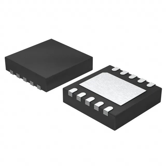
Single low-side gate driver with 8A sink capability for automotive power stages
It delivers a peak output of 4A source and 8A sink, which directly determines the gate charge transfer rate and therefore the MOSFET switching losses and cross-conduction margin. The part accepts a supply voltage from 4.5V to 28V, covering 5V logic rails, 12V automotive battery lines, and 24V industrial buses without requiring an external regulator. Both inverting and non-inverting input logic is available on the same die, giving the designer flexibility to match the controller's PWM polarity without adding an inverter gate.
AEC-Q100 qualification and 150°C junction temperature
For industrial applications, the same temperature margin provides derating headroom in motor-drive enclosures and outdoor telecom power supplies.
Supply rail and logic-level compatibility
The 4.5V to 28V supply range means this driver can run directly from a 5V bias rail, a 12V battery, or a 24V industrial bus. The logic input thresholds are specified at VIL = 0.8V and VIH = 2.0V, which are compatible with 3.3V and 5V logic families from MCUs and DSPs. No level-shifter is needed between the controller and the driver input for these common logic voltages. The rise and fall times of 22ns and 16ns typical, combined with the 8A sink current, allow fast turn-off of the power MOSFET, reducing the dead-time requirement in half-bridge topologies.
The 10-WFDFN package with exposed pad (10-TDFN, 3x3mm) is a surface-mount design that relies on the PCB copper plane for heat spreading. The small footprint (3x3mm) suits space-constrained modules like on-board chargers and DC-DC converters in automotive ECUs.