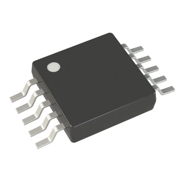
High-side gate driver for N-channel MOSFETs — 60 V bootstrap ceiling
The LTC7004HMSE#TRPBF is a single-channel, non-inverting high-side gate driver from Analog Devices, designed to drive an N-channel MOSFET. It operates from a 3.5 V to 15 V supply and can float up to a 60 V bootstrap voltage, meaning the driven MOSFET's drain can sit at up to 60 V above ground while the driver's supply stays referenced to the source pin. This is the part you pick when you need to switch a 12 V, 24 V, or 48 V rail on the high side with a single N-channel FET and want the gate drive amplitude to be independent of the rail voltage.
90 ns rise, 40 ns fall — switching speed and the thermal trade-off
Typical rise time of 90 ns and fall time of 40 ns put the LTC7004 in the medium-speed class for a high-side driver. The asymmetric fall is faster than the rise, which helps by turning the MOSFET off more quickly than it turns on — a common design pattern to minimize shoot-through in half-bridge or synchronous rectifier stages. For a 12 V automotive load switching at 20 kHz to 100 kHz, these edges are clean enough to keep switching losses manageable without requiring aggressive gate resistors to slow the turn-on for EMI control. If you are driving a large-capacitance FET (several nF of input capacitance), the 90 ns rise will stretch; budget for that in the dead-time or switching-loss calculation.
This is the extended industrial / automotive range — the 150°C upper limit means it can sit next to a hot MOSFET on a power board in an engine bay, a solar inverter, or a motor drive enclosure without derating. Plan for a minimum of four vias under the pad, tied to an inner-layer ground plane.
The ROHS3 compliance is current and covers the EU recast directive.