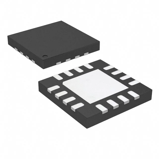
Analog Devices LTC3851AEUD-1#PBF — Discrete Semiconductors

LTC3851AEUD-1#PBF Buck Controller, 235-750kHz, 16-QFN

MPNLTC3851AEUD-1#PBF
End of Life

Analog Devices LTC3851AEUD-1#PBF synchronous buck controller, step-down topology, 4V to 38V supply, 235kHz to 750kHz switching, transistor driver output, 16-WFQFN exposed pad package, tube.

$5.87Ref. price · indicative, final on quote
Packaging16-WFQFN Exposed Pad
RoHSROHS3 Compliant
Sourced new & surplus through independent channelsAuthenticity-screened · ESD-safe packingListing updated Aug 2026

Specifications

LTC3851AEUD-1#PBF specifications
ParameterValue
Output typeTransistor Driver
MountingSurface Mount
Voltage - supply (Vcc (Vdd))4V ~ 38V
Frequency235kHz ~ 750kHz
I/O channels1
Output phases1
Duty cycle99%
Operating temperature-40°C ~ 125°C (TJ)
PackageTube
FunctionStep-Down
TopologyBuck
Clock syncNo
Case16-WFQFN Exposed Pad
Control featuresEnable, Frequency Control, Power Good, Soft Start, Tracking
Output configurationPositive
Synchronous rectifierYes

Product details

Synchronous buck controller with wide input range

The LTC3851AEUD-1#PBF is a single-phase synchronous buck controller from Analog Devices, designed for step-down conversion from input rails spanning 4V to 38V (Vcc/Vdd). The 99% maximum duty cycle means it can run near dropout — useful when the input sags close to the output target, like in battery-backed systems where the bus voltage decays under load. Switching frequency is programmable from 235kHz to 750kHz via a resistor on the RT pin. The lower end suits designs prioritising efficiency (lower FET gate-charge losses), while the upper end shrinks the inductor and output capacitor footprint. There is no clock-sync input on this variant — the -1 suffix omits that feature, so if you need external synchronisation to a system clock, look at the LTC3851EUFD or similar parts with SYNC capability.

Package, thermal, and board-fit

Housed in a 16-lead WFQFN with exposed pad (3x3 mm body, supplier device package 16-QFN). The 0.5 mm pitch QFN demands careful solder-paste stencil design; a 4-layer board with thermal vias under the pad is standard practice for this package class. Control features include Enable, Frequency Control, Power Good, Soft Start, and Tracking. The tracking input lets the output voltage follow an external ramp during startup — useful for sequencing multiple rails in an FPGA or SoC power tree. Output configuration is positive, and the transistor driver output drives external N-channel MOSFETs in a synchronous rectifier topology.

Frequently asked questions

Will LTC3851AEUD-1#PBF drop into a board designed for LTC3851EMSE-1#PBF without rewiring?

No — the packages are different. LTC3851AEUD-1#PBF is a 16-QFN (3x3 mm) with exposed pad, while LTC3851EMSE-1#PBF uses an MSOP-16E package. The pinouts and footprint are not compatible; a board layout change is required.

What is the switching frequency range of LTC3851AEUD-1#PBF?

The switching frequency is programmable from 235kHz to 750kHz via an external resistor on the RT pin. There is no clock-sync input on this variant.