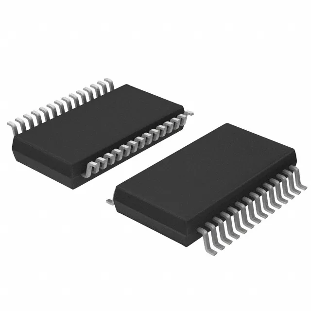
Boost controller with synchronous rectification
The LTC3813EG#PBF: The synchronous rectifier architecture replaces the traditional boost diode with a second FET, cutting conduction losses in the rectification path and improving efficiency at higher output currents. Operating from a 6.35 V to 14 V bias supply (Vcc/Vdd), the controller generates a regulated output through a single-phase, positive-output transistor driver. The 1-output configuration suits point-of-load rails that need a voltage higher than the input bus — common in telecom backplanes, battery-powered systems, and automotive pre-boost stages.
Control features and clock sync
On-chip control features include Enable, Power Good flag, and Soft Start. The Power Good output monitors the regulated rail and can sequence downstream converters or reset a microcontroller on power-up. Soft Start ramps the output voltage gradually, limiting inrush current from the input supply during start-up. The clock synchronization input (Clock Sync = Yes) lets the controller lock to an external clock signal, shifting the switching frequency away from sensitive bands in RF or instrumentation systems. Without an external clock, the part runs from its internal oscillator; with one, multiple converters can be phase-aligned to reduce input ripple current.