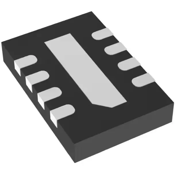
Dual 300 mA buck in a 3x2 mm DFN
The LTC3547EDDB#TRPBF: The adjustable output can be set as low as 0.6 V via an external resistor divider, covering the core voltages for most low-power MCUs and RF SoCs. Switching at 2.25 MHz keeps the inductor and output capacitor small — a 2.2 µH inductor and 10 µF ceramic cap are typical for each channel. The synchronous rectifier eliminates the external Schottky diode, saving board area and improving efficiency across the load range.
Package and board-fit — exposed pad matters
Housed in an 8-lead WFDFN with exposed pad (3 mm × 2 mm body, 0.50 mm pitch), the LTC3547EDDB#TRPBF requires a thermal land on the PCB to sink heat from the die. No AEC-Q grade is listed, so this part is not qualified for under-hood automotive use.