Package and integration story
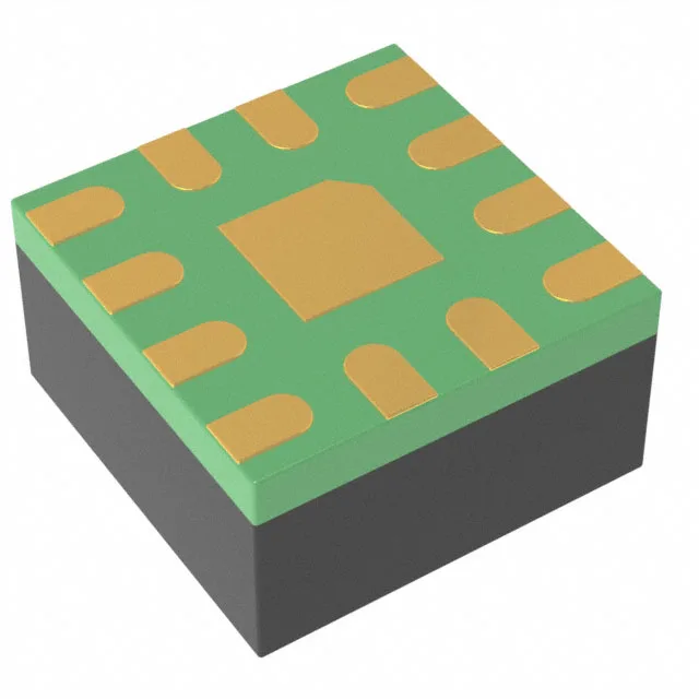
The LTC3315AACBZ-R7 packs two independent 2 A buck converters into a 16-bump WLCSP measuring 1.64x1.64 mm — the smallest footprint for a dual 2 A rail in the automotive temperature range. The 0.4 mm pitch WLCSP demands a controlled solder-paste stencil and a reflow profile matched to the 0.3 mm bump height; the exposed backside is the die itself, so the board's top-layer copper plane under the package acts as the primary heat spreader. Each channel delivers 2 A continuous from a 2.25 V to 5.5 V input rail, covering 3.3 V and 5 V system buses with margin for automotive cold-crank dips down to 2.25 V. The 2 MHz fixed switching frequency keeps the inductor in the 0.47 µH to 2.2 µH range — small enough for a 0603 footprint — but the loop compensation is internal, so the output capacitor ESR and ESL must stay within the datasheet's stable region to avoid sub-harmonic oscillation at heavy load.
AEC-Q100 grade and the under-hood thermal profile
Qualified to AEC-Q100 Grade 1 with a junction temperature range of -40°C to 125°C — this is the full under-hood envelope. The 125°C TJ limit means the part can sit next to an engine block or inside a transmission ECU without derating the output current, provided the board's thermal impedance keeps the die below that ceiling. The synchronous rectifier (integrated low-side FET) reduces the external component count but shifts the thermal dissipation into the package; at 2 A per channel with a 3.3 V to 1.8 V conversion, the junction rise is roughly 40°C above ambient in still air, leaving 85°C ambient headroom before hitting the 125°C limit.
Layout checklist for the WLCSP footprint
The 16-WLCSP with 0.4 mm pitch and 0.3 mm bump diameter requires a solder-mask-defined pad of 0.22 mm diameter on the board. Via-in-pad is not recommended — the solder wicks into the via and starves the bump joint. Instead, route the output and input traces on the top layer to the nearest via array, keeping the high-current paths (VIN, SW, VOUT) under 5 mm before dropping to an inner layer. The two channels share a common VIN pin; the input decoupling capacitor (10 µF X7R per channel) must sit within 2 mm of the VIN-GND bump pair to keep the input ripple below 50 mV at 2 A load step. The adjustable output voltage is set by a resistor divider from VOUT to the FB pin. The FB pin threshold is 0.5 V (the minimum output voltage), so for a 1.8 V output the top resistor is 130 kΩ and the bottom is 49.9 kΩ — standard E96 values. The FB trace should be kept under 10 mm and shielded from the SW node by a ground pour to avoid noise injection into the feedback loop.