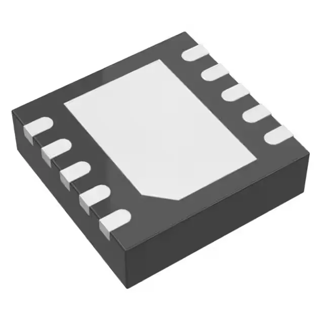
500 mA step-up charge pump in a 3x3 mm DFN
The LTC3203EDD#PBF: It generates a positive output adjustable from 0.91 V up to 5 V — covering single-cell Li-Ion to 5 V logic rails, and also suiting 1.8 V core supplies from the 0.91 V minimum. The charge-pump topology means lower conducted and radiated noise than a switching inductor at the same load, making it a fit for powering analog front-ends, sensor bias, or RF VCOs where ripple on the supply rail directly degrades signal integrity.
Dual switching frequency — 900 kHz or 1 MHz
The switching frequency is pin-selectable between 900 kHz and 1 MHz. At 1 MHz the external flying capacitors and output capacitor can be smaller (lower profile, cheaper), while 900 kHz reduces switching losses at light loads — useful when the 500 mA rating is only hit in short bursts. No synchronous rectifier is used, so the Schottky diode's forward voltage adds to the dropout — budget about 0.4 V at 500 mA. The efficiency peak sits around 200-300 mA; above that the diode conduction loss dominates.
10-lead DFN with exposed pad — hand-solderable
The tube packaging is fine for prototype reels, but for volume production you will want the tape-and-reel variant (LTC3203EDD#TRPBF) to feed a pick-and-place.