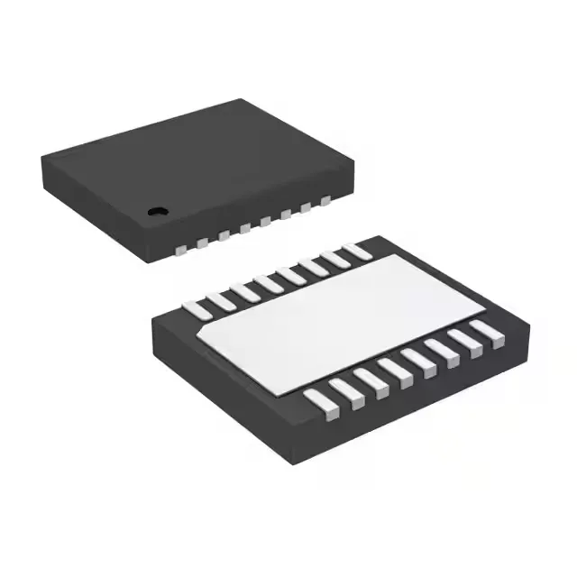
Analog Devices LTC3113EDHD#PBF — Discrete Semiconductors

LTC3113EDHD#PBF Buck-Boost Regulator, 3 A, Adjustable

MPNLTC3113EDHD#PBF
End of Life

Analog Devices LTC3113EDHD#PBF buck-boost switching regulator, 3 A output, adjustable 1.8-5.5 V, 300 kHz-2 MHz, synchronous rectification, 16-WFDFN exposed pad, tube.

$11.91Ref. price · indicative, final on quote
Packaging16-WFDFN Exposed Pad
RoHSROHS3 Compliant
Sourced new & surplus through independent channelsAuthenticity-screened · ESD-safe packingListing updated Aug 2026

Specifications

LTC3113EDHD#PBF specifications
ParameterValue
Output typeAdjustable
MountingSurface Mount
Voltage - input5.5V
Voltage - output5.5V
Voltage - output (Min (Fixed))1.8V
Output current3A
Frequency300kHz ~ 2MHz
I/O channels1
Operating temperature-40°C ~ 125°C (TJ)
PackageTube
FunctionStep-Up/Step-Down
TopologyBuck-Boost
Case16-WFDFN Exposed Pad
Output configurationPositive
Synchronous rectifierYes

Product details

3 A buck-boost regulator with synchronous rectification

The LTC3113EDHD#PBF: This is a single-inductor buck-boost converter delivering 3 A continuous output. The topology regulates the output voltage above, below, or equal to the input — useful for battery-powered systems where the cell voltage drops below the regulated rail. The synchronous rectifier (internal low-side FET) replaces the external catch diode typical in non-synchronous designs, reducing the conduction loss and component count. Efficiency benefits most at lower output voltages where the diode forward drop would otherwise dominate.

Input range and switching frequency flexibility

The minimum 1.8 V input means the regulator can continue delivering a regulated 3.3 V output even as the battery discharges below 2 V. Switching frequency is programmable from 300 kHz to 2 MHz via an external resistor. Lower frequencies improve efficiency by reducing switching losses; higher frequencies shrink the inductor footprint at the cost of increased FET switching losses and core loss in the magnetics. The positive output configuration and single-output channel suit point-of-load regulation for FPGAs, sensors, or RF power amplifiers requiring a clean, regulated rail above or below the input.

The 16-lead WFDFN package with an exposed thermal pad (supplier device package 16-DFN 5x4 mm) requires the pad to be soldered to a PCB copper plane for thermal dissipation. At 3 A output, the power loss (I² × Rds(on) + switching losses) can exceed 1.5 W; the board copper area and via array under the pad set the effective thermal resistance.

Frequently asked questions

What is the output current rating of the LTC3113EDHD#PBF?

The regulator delivers 3 A continuous output. This rating assumes proper thermal management via the exposed pad — the actual achievable current depends on the PCB copper area, ambient temperature, and airflow.

What input voltage range does the LTC3113EDHD#PBF support?

The buck-boost topology allows the output to be set above, below, or equal to the input, so it can regulate a 3.3 V rail from a Li-Ion battery that discharges from 4.2 V down to 2.5 V.

What package does the LTC3113EDHD#PBF come in?

It is supplied in a 16-lead WFDFN package with an exposed thermal pad, measuring 5 mm × 4 mm (supplier device package 16-DFN). The tube packaging is the standard shipping medium for this order code.