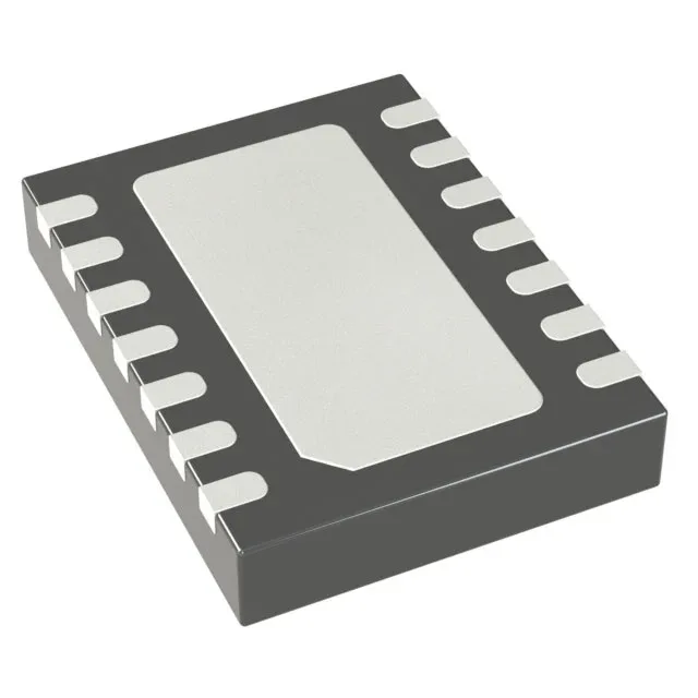
Analog Devices LTC2637IDE-LZ8#PBF — Discrete Semiconductors

LTC2637IDE-LZ8#PBF 8-bit DAC, 8-channel I²C, 14-DFN

MPNLTC2637IDE-LZ8#PBF
End of Life

Analog Devices LTC2637IDE-LZ8#PBF, 8-bit octal DAC, voltage-buffered output, I²C interface, 3.5µs settling time, 14-WFDFN exposed pad, tube package.

$9.97Ref. price · indicative, final on quote
Packaging14-WFDFN Exposed Pad
RoHSROHS3 Compliant
Sourced new & surplus through independent channelsAuthenticity-screened · ESD-safe packingListing updated Aug 2026

Specifications

LTC2637IDE-LZ8#PBF specifications
ParameterValue
Output typeVoltage - Buffered
MountingSurface Mount
Reference typeExternal, Internal
Voltage - supply, analog2.7V ~ 5.5V
Voltage - supply, digital2.7V ~ 5.5V
InterfaceI²C
Operating temperature-40°C ~ 85°C
PackageTube
INL (DNL)±0.05, ±0.5 (Max)
Settling time3.5µs (Typ)
Number of bits8
Case14-WFDFN Exposed Pad
Differential outputNo
Number of d (A converters)8

Product details

Eight channels on a single I²C bus

The LTC2637IDE-LZ8#PBF packs eight 8-bit DACs with voltage-buffered outputs into a 14-DFN package, each channel individually addressable over a single I²C bus. That means you can set eight analog voltages — bias levels, setpoints, trim voltages — without multiplying the bus load or the board area. Settling to 8-bit accuracy in 3.5 µs typical, the part handles per-channel updates fast enough for closed-loop trim loops or dynamic bias adjustment in a multi-channel system.

Supply rails and reference flexibility

The reference can be either the internal 2.5 V bandgap or an external voltage applied to the REF pin, giving you a choice between a self-contained calibration source and a ratiometric system reference. The 14-WFDFN exposed-pad package (4x3 mm body) needs a thermal via under the pad for heat sinking if the part is driving heavy DC loads on all eight channels simultaneously. For typical trim applications the pad can be tied to ground without a via.

INL and DNL — what the numbers mean for your setpoint

Integral nonlinearity is ±0.05 LSB typical, ±0.5 LSB maximum at 8-bit resolution. That means the worst-case deviation from the ideal transfer line is half an LSB — about 20 mV on a 5 V reference. Differential nonlinearity is ±0.5 LSB max, guaranteeing monotonicity: every code step produces a positive output increment, so the DAC never skips a voltage.

Active production and compliance

It is ROHS3 compliant, so it passes the current EU restriction directive without exemption claims. For extended temperature requirements (105°C or 125°C), the AD5308ARUZ sibling runs to 125°C but uses an SPI interface and a different package.

Frequently asked questions

What is the closest functional second-source to LTC2637IDE-LZ8#PBF?

The AD5645RBRUZ is a 14-bit, 4-channel I²C DAC in a different package — not a pin-to-pin drop-in. The AD5308ARUZ is an 8-bit, 8-channel SPI part that matches the channel count and resolution but uses a serial peripheral interface instead of I²C. Neither is a direct replacement without a board spin or bus change.

Will LTC2637IDE-LZ8#PBF drop into a board designed for AD5645RBRUZ?

No — the AD5645RBRUZ is a 14-bit, 4-channel part in a 14-TSSOP package, while the LTC2637IDE-LZ8#PBF is an 8-bit, 8-channel part in a 14-DFN. The pinouts and channel counts differ; a new layout is required.

What compliance documentation does Analog Devices provide for LTC2637IDE-LZ8#PBF?

The part is ROHS3 compliant per the manufacturer's declaration.