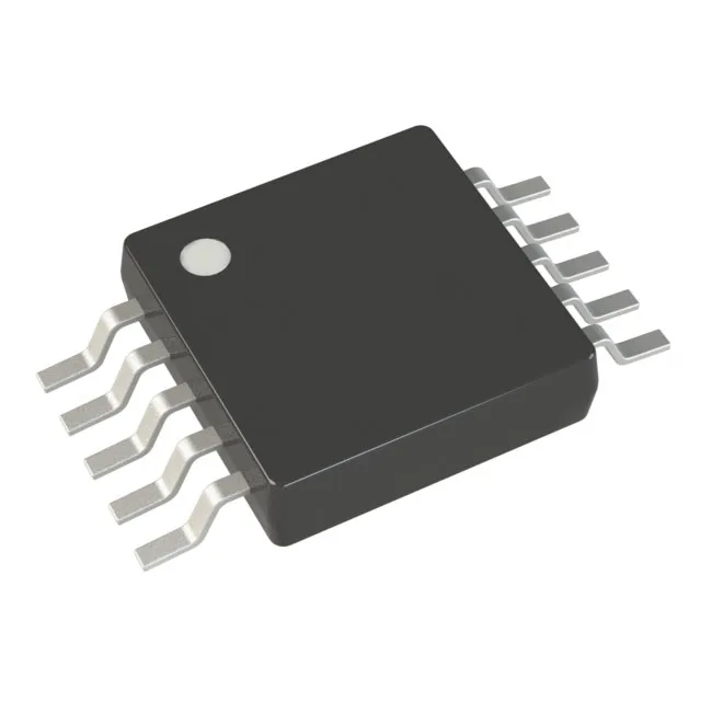
Analog Devices LTC2634CMSE-HZ12#PBF — Discrete Semiconductors

LTC2634CMSE-HZ12#PBF 12-bit Quad DAC, SPI, 10-MSOP-EP

MPNLTC2634CMSE-HZ12#PBF
End of Life

Analog Devices LTC2634CMSE-HZ12#PBF, 12-bit quad DAC, buffered voltage output, SPI interface, 4.8µs settling time, ±1 LSB INL/DNL, 10-MSOP-EP package, Tube.

$10.9Ref. price · indicative, final on quote
Packaging10-TFSOP, 10-MSOP (0.118", 3.00mm Width) Exposed Pad
RoHSROHS3 Compliant
Sourced new & surplus through independent channelsAuthenticity-screened · ESD-safe packingListing updated Aug 2026

Specifications

LTC2634CMSE-HZ12#PBF specifications
ParameterValue
Output typeVoltage - Buffered
MountingSurface Mount
Reference typeExternal, Internal
Voltage - supply, analog5V
Voltage - supply, digital5V
InterfaceSPI
Operating temperature0°C ~ 70°C
PackageTube
INL (DNL)±1, ±1 (Max)
Settling time4.8µs (Typ)
Number of bits12
Case10-TFSOP, 10-MSOP (0.118\", 3.00mm Width) Exposed Pad
Differential outputNo
Number of d (A converters)4

Product details

12-bit quad DAC in a compact exposed-pad package

The LTC2634CMSE-HZ12#PBF is a 12-bit quad digital-to-analog converter from Analog Devices, packing four independent buffered voltage outputs into a 10-MSOP-EP package. It communicates over an SPI interface and settles to within 1 LSB in 4.8µs typical — fast enough for closed-loop control or multi-channel waveform generation in a compact footprint.

Package and board-fit: the exposed pad matters

The 0.118-inch (3.00 mm) body width is standard MSOP-10 footprint, but the exposed pad adds a center pad that needs a matching soldermask opening.

Supply rails and reference: single 5V operation

Both analog and digital supplies run from a single 5V rail (5V for VDD and DVDD), simplifying the power tree — no split supply needed. The reference can be external or internal, giving flexibility: use the internal reference for standalone operation or drive an external reference for ratiometric accuracy against a system voltage.

Temperature range and accuracy

INL and DNL are ±1 LSB max each, meaning monotonicity is guaranteed and the transfer function stays within 1 LSB of ideal across the full output range.

Frequently asked questions

What is the output type and interface of this DAC?

It has a buffered voltage output (not current or unbuffered) and uses an SPI serial interface. The buffered output can drive moderate loads directly without an external op-amp.