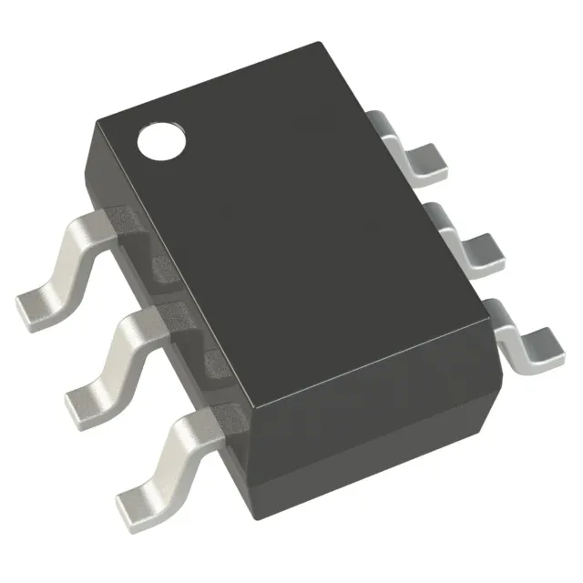
10-bit DAC with SPI for precision trim and control loops
The LTC2630CSC6-HZ10#TRMPBF is a single-channel 10-bit digital-to-analog converter with a buffered voltage output and an SPI-compatible serial interface. With a typical settling time of 4.4 µs to ±0.5 LSB, this DAC can update at rates exceeding 200 kHz, making it suitable for closed-loop control and real-time calibration in industrial and instrumentation systems.
Linearity and monotonicity for calibration-grade output
The integral non-linearity (INL) is ±0.2 LSB typical and ±0.5 LSB maximum, while the differential non-linearity (DNL) is ±0.5 LSB maximum. These figures guarantee monotonic performance across the full 10-bit range — every code step produces a positive voltage increment, essential for trimming power supplies or sensor offsets. The buffered output can source or sink current without an external op-amp, though the load current affects settling time. For a 2 kΩ load with 100 pF capacitance, the 4.4 µs typical settling still holds; heavier loads may need a buffer.
Package, supply, and temperature grade for BOM fit
Housed in a 6-lead SC-70 package (also known as SOT-363), the device occupies roughly 2 mm × 2 mm of board area. The 0.65 mm pin pitch is layout-friendly for two-layer boards. The analog and digital supply rails share a single 5 V pin — no split-plane routing needed.