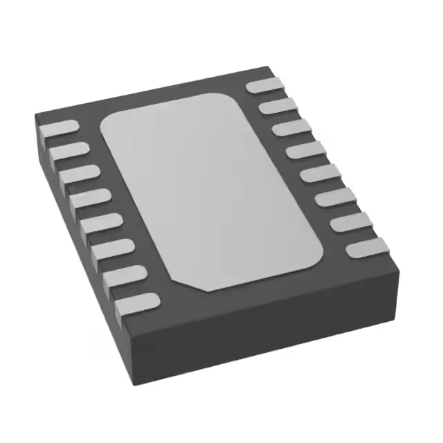
18-bit SAR ADC in a 4x3 mm DFN — what the package and pinout mean for the board
The LTC2378IDE-18#PBF is an 18-bit successive-approximation-register (SAR) ADC from Analog Devices, sampling at 1 Msps with a single differential input. The 16-lead WFDFN with exposed pad (4x3 mm) is the kind of package a rework tech can handle with hot air if the board layout gives the pad room — the exposed paddle needs a solid thermal via array under it to pull heat away from the die during conversion bursts.
1 Msps throughput with external reference — the signal chain fit
At 1 Msps the SAR core needs a clean 2.375 V to 2.625 V analog supply and a separate digital rail in the same range — both rails should be low-noise LDOs, not switching regulators, because the internal comparator sees every ripple as a conversion error. The external reference (not included on-chip) sets the full-scale range; a 2.5 V reference like the ADR4525 gives a 5 Vpp differential input swing when the analog supply is 2.5 V. The SPI interface runs at up to 50 MHz typical for the serial clock, so the digital lines can be routed through a header or directly to a controller without a level shifter as long as the host side matches the 2.5 V logic level. The 1:1 S/H-to-ADC ratio means the sample-and-hold capacitor charges directly from the input during the acquisition phase — the source impedance driving the differential inputs should stay under 100 Ω to settle within 300 ns at 1 Msps.