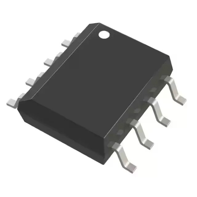
Dual independent gate driver for N-channel MOSFETs
The LTC1693-2CS8#PBF is a dual independent gate driver from Analog Devices, designed to drive N-channel MOSFETs in either high-side or low-side configuration. With two independent channels, it can control separate MOSFETs or drive a half-bridge pair, each channel offering 1.5 A peak source and sink current — enough to charge and discharge the gate capacitance of medium-power FETs in tens of nanoseconds.
Switching speed and drive strength
Typical rise and fall times are 16 ns each into a standard load — this 16 ns, 16 ns symmetry means the turn-on and turn-off delays are balanced, which simplifies dead-time calculation in a half-bridge. The 1.5 A peak output (both source and sink) provides the current slew rate needed to overcome the Miller plateau of a large-gate-charge MOSFET without excessive switching loss. Supply voltage range is 4.5 V to 13.2 V, covering common logic rails (5 V) and bias rails (12 V) used in industrial and telecom power supplies. The logic input thresholds are 1.7 V (VIL) and 2.2 V (VIH), so the driver accepts 3.3 V logic directly without a level shifter.
Package and temperature grade
The operating junction temperature range is 0°C to 150°C, making it appropriate for commercial and industrial environments where ambient temperatures stay below 85°C but the die may see higher temperatures under load. The input type accepts both inverting and non-inverting signals on the same channel — the LTC1693-2 variant provides this flexibility, allowing the designer to choose the polarity that matches the PWM controller output without external inversion.
The part is supplied in tube packaging, suitable for prototype and low-to-medium volume assembly.