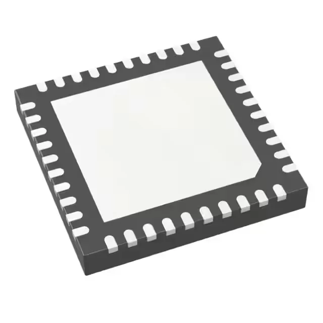
Four-rail power tree in one 6x6 mm package
The LT8602EUJ#TRPBF is a quad-output step-down buck regulator from Analog Devices, packing four independent switching rails into a 40-WFQFN exposed pad package measuring 6x6 mm. It replaces the board area and BOM count of four separate single-channel regulators where the load currents fit the mixed 1.5 A, 1.8 A, and 2.5 A output ratings. The input voltage range spans 2.6 V to 42 V, covering automotive battery rails (12 V nominal, cold-crank down to 4.5 V, load-dump up to 40 V) and industrial 24 V bus supplies without an external pre-regulator. Each output is adjustable from a 0.8 V or 1 V minimum reference up to 42 V, limited by the input rail.
Switching frequency and inductor selection
The switching frequency is programmable from 250 kHz to 2.2 MHz via a single resistor. A lower frequency reduces switching losses and improves efficiency at light load but demands a larger inductor; a higher frequency shrinks the inductor footprint at the cost of higher FET switching losses and tighter thermal margin in the 40-QFN package.
Temperature grade and deployment context
The exposed pad (40-WFQFN, 6x6 mm) must be soldered to a thermal land on the PCB to keep the junction below the 125°C absolute maximum under full load.