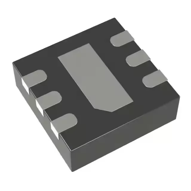
4.096V precision reference — 1.5µA supply current defines the use case
The LT6656AIDC-4.096#TRMPBF is a series voltage reference from Analog Devices that outputs a fixed 4.096V with ±0.1% initial tolerance. Its headline draw is 1.5µA supply current — low enough that the reference itself doesn't dominate the power budget in a battery-powered sensor node or portable instrument that stays on continuously. Input range spans 4.596V to 18V, so it runs from a 5V rail with 0.4V headroom or straight off a 12V supply without a pre-regulator. The 5 mA output current is enough to drive an ADC reference input and its decoupling capacitor without an external buffer.
Noise floor and temperature drift — what the numbers mean on the bench
For a 4.096V output, that works out to roughly 123 µVp-p — relevant when the reference feeds a 16-bit or 18-bit ADC where the LSB at 4.096V full-scale is 62.5 µV or 15.6 µV respectively. The noise sits below the LSB for 16-bit conversions but starts to eat into the noise budget at higher resolutions. Over a 125°C span, the output drifts by up to 5.12 mV — about 0.125% of the 4.096V set point. That's tight enough for 12-bit absolute accuracy across temperature but needs calibration for 16-bit systems that hold accuracy over the full temperature window.
Package, mounting, and board integration
The 6-WFDFN exposed pad package measures 2x2 mm (supplier device package 6-DFN). The exposed pad on the underside must be soldered to a PCB thermal land — it carries the ground connection and pulls heat out of the die. Without a proper thermal via array under the pad, the junction temperature rises faster than the datasheet's thermal resistance assumes.
Lifecycle and compliance — active, no obsolescence concern
ROHS3 compliant per the manufacturer's declaration.