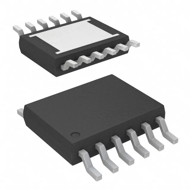
Analog Devices LT3652EMSE#PBF — Power Management (PMIC / Gate Driver)

LT3652EMSE#PBF Analog Devices Battery Charger IC, 2A

MPNLT3652EMSE#PBF
End of Life

Analog Devices LT3652EMSE#PBF multi-chemistry battery charger IC, 2A max charge current, 14.4V battery pack voltage, 32V supply max, 12-TSSOP exposed pad, tube, surface mount.

$9.23Ref. price · indicative, final on quote
Packaging12-TSSOP (0.118", 3.00mm Width) Exposed Pad
RoHSROHS3 Compliant
Sourced new & surplus through independent channelsAuthenticity-screened · ESD-safe packingListing updated Aug 2026

Specifications

LT3652EMSE#PBF specifications
ParameterValue
MountingSurface Mount
Battery pack voltage14.4V
Voltage32V
Current - chargingConstant - Programmable
Charge current - max2A
Operating temperature-40°C ~ 125°C (TJ)
PackageTube
Case12-TSSOP (0.118\", 3.00mm Width) Exposed Pad
Battery chemistryMulti-Chemistry
Programmable featuresCurrent, Timer

Product details

Multi-chemistry charger with programmable current and timer

The LT3652EMSE#PBF is a multi-chemistry battery charger IC from Analog Devices, handling Li-Ion, Li-Polymer, NiMH, and NiCd chemistries through a constant-current/constant-voltage algorithm. The 2 A max charge current and 14.4 V battery pack voltage ceiling make it a fit for charging 4-series Li-Ion packs or sealed lead-acid batteries at moderate current. Supply voltage tolerance up to 32 V means the part can regulate from unregulated wall adapters or automotive rails without an external pre-regulator — the input range absorbs transients common in 12 V and 24 V systems.

Package and thermal management

Housed in a 12-TSSOP package with an exposed pad (0.118" width, 3.00 mm), the LT3652EMSE#PBF relies on the thermal pad soldered to a PCB copper plane to dissipate heat during high-current charging. The exposed pad is the primary thermal path — a layout without a solid ground-plane connection under the pad will limit the charge current before the 2 A ceiling is reached. The supplier device package is 12-MSOP-EP, functionally identical to the 12-TSSOP-EP footprint. Both refer to the same 3 mm × 3 mm body with an exposed pad; the MSOP and TSSOP nomenclatures are interchangeable for this part's land pattern.

Temperature grade and charging control

The wide junction range means the charger can run at full 2 A current into a hot battery without hitting thermal shutdown, provided the PCB copper area is adequate. Programmable features include charge current set by an external resistor and a safety timer that terminates charging if the battery does not reach full voltage within the programmed window. The timer prevents overcharging a failed cell that never reaches termination voltage.

Lifecycle and compliance

Sourced to order against BOM quantities.

Frequently asked questions

How can I order LT3652EMSE#PBF or check availability?

Submit an RFQ for lot-specific date codes and packaging condition.

What is the difference between LT3652EMSE#PBF and LT3652IMSE#PBF?

Both parts share the same multi-chemistry charger core, 2 A max charge current, 14.4 V pack voltage, and 12-MSOP-EP package. The 'E' vs 'I' suffix denotes the temperature screening level, not a parametric difference.

Will LT3652EMSE#PBF drop into a board designed for LT3652EDD#PBF?

No — the LT3652EDD#PBF uses a 12-DFN (3 mm × 3 mm) package with a different footprint and thermal pad layout. The LT3652EMSE#PBF is a 12-MSOP-EP (TSSOP) package. The two are not pin-to-pin compatible; a board spin is required to swap between them.

What compliance documentation does Analog Devices provide for LT3652EMSE#PBF?

Analog Devices provides RoHS3 compliance certification and a material declaration per the EU RoHS directive. The ROHS3 compliance is confirmed on the product status.