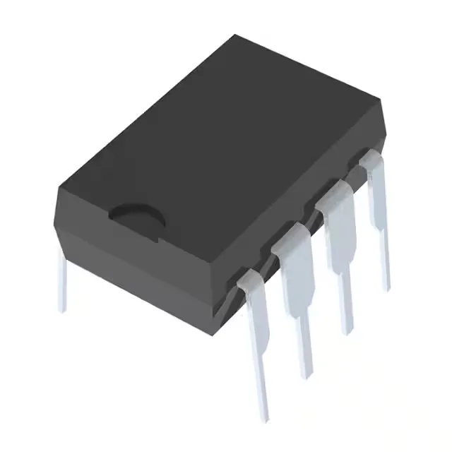
Analog Devices LT1457CN8#PBF — Analog & Data Acquisition

LT1457CN8#PBF JFET Op Amp, Dual, 4V/µs Slew Rate, 8-DIP

MPNLT1457CN8#PBF
End of Life

Analog Devices LT® series, LT1457CN8#PBF, dual JFET operational amplifier, 1.7 MHz gain bandwidth, 4V/µs slew rate, 7 pA input bias, 200 µV offset, 1.8 mA supply (two channels), 9–36 V supply span, through-hole 8-DIP (0.300"), -40°C to 85°C.

$6.33Ref. price · indicative, final on quote
Packaging8-DIP (0.300", 7.62mm)
RoHSROHS3 Compliant
SeriesLT®
Sourced new & surplus through independent channelsAuthenticity-screened · ESD-safe packingListing updated Aug 2026

Specifications

LT1457CN8#PBF specifications
ParameterValue
SeriesLT®
MountingThrough Hole
Amplifier typeJ-FET
Voltage - input offset200 µV
Voltage - supply span36 V
Current - supply1.8mA (x2 Channels)
Current - input bias7 pA
Operating temperature-40°C ~ 85°C
Gain bandwidth product1.7 MHz
PackageTube
Slew rate4V/µs
Case8-DIP (0.300\", 7.62mm)
Number of circuits2

Product details

Dual JFET op amp for precision analog front-ends

The LT1457CN8#PBF is a dual JFET-input operational amplifier from Analog Devices' LT® series, packaged in a through-hole 8-DIP (0.300", 7.62mm).

Sourcing and lifecycle — active, no LTB pressure

What the key ratings mean for the BOM

The 4V/µs slew rate and 1.7 MHz GBW set the usable bandwidth. The 7 pA input bias and 200 µV offset are the precision specs that matter for DC accuracy.

Package and integration — through-hole DIP

The 8-DIP (0.300", 7.62mm) body is the standard dual-in-line footprint. Through-hole mounting suits prototyping and rework.

Frequently asked questions

Where can I buy LT1457CN8#PBF?

The LT1457CN8#PBF is available to order through independent semiconductor distribution. Submit an RFQ for current pricing and availability — stock levels and lead times are confirmed at quote time, not listed on the page.

Is LT1457CN8#PBF a dual op amp?

Yes, it is a dual JFET operational amplifier with two independent channels in a single 8-pin DIP package.

What are the alternative or equivalent parts to LT1457CN8#PBF?

A close functional peer is the AD712KNZ, also a dual JFET op amp in a through-hole DIP. The AD712 offers a 4 MHz GBW and 20 V/µs slew rate, but its input offset voltage is 300 µV and it is specified only for 0°C to 70°C — not the full industrial -40°C to 85°C range of the LT1457CN8#PBF. For a wider temperature range (-40°C to 125°C) and lower bias (2 pA), the ADA4062-4ARUZ is a quad surface-mount option, though its 1.4 MHz GBW and 3.3 V/µs slew rate are slightly lower. Neither is a drop-in replacement without verifying the pinout and supply voltage.

What is the pinout of LT1457CN8#PBF?

Standard 8-DIP dual op amp pinout: pin 1 = Output A, pin 2 = Inverting Input A, pin 3 = Non-Inverting Input A, pin 4 = V–, pin 5 = Non-Inverting Input B, pin 6 = Inverting Input B, pin 7 = Output B, pin 8 = V+.