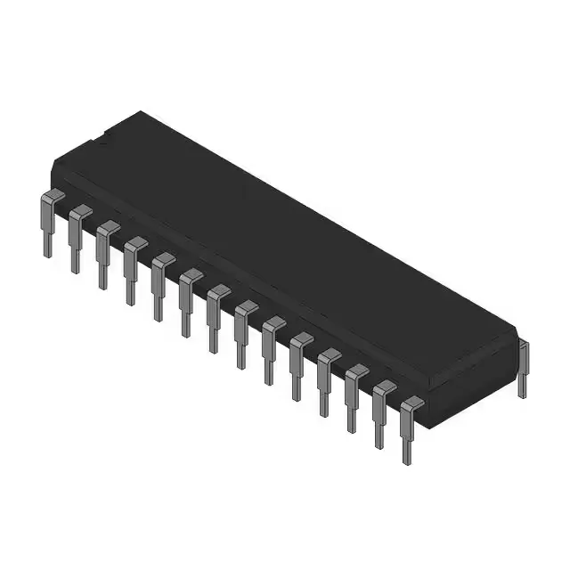
24-bit triple DAC in a through-hole PDIP
The ADV7146KN50 is a 24-bit triple D/A converter from the ADV7146 series, described as a continuous edge graphics RAM-DAC. It integrates three independent DACs on one die, each with a buffered voltage output, and is packaged in a 28-pin PDIP (0.600-inch body width, 15.24 mm pitch) for through-hole assembly. This part targets applications where three analog voltage channels must be generated from a digital stream — think RGB video lookup tables, arbitrary waveform generation, or multi-channel programmable voltage references — all from a single IC footprint.
Dual 5 V rails and commercial temperature range
This split-plane architecture keeps digital switching noise from coupling into the analog output path — the nominal 5 V supply is the same for both, but the PCB layout must decouple each plane independently to maintain the ±1 LSB INL/DNL spec. It is not specified for extended industrial or automotive temperature ranges — a board that sees 85°C inside an enclosure will exceed the operating limit.
Peer cross-reference — AD569KNZ
The ADV7146KN50 offers 24-bit resolution and three DACs versus the AD569's single 16-bit channel, but both share a through-hole PDIP package and buffered voltage output topology. The AD569KNZ uses a segmented DAC architecture with ±0.020 LSB INL and ±0.5 LSB DNL, a tighter linearity spec than the ADV7146's ±1 LSB, but at 16 bits versus 24. For a design that needs three channels, the ADV7146KN50 replaces one AD569 plus two additional single-channel DACs — a board-area and BOM-count trade-off.